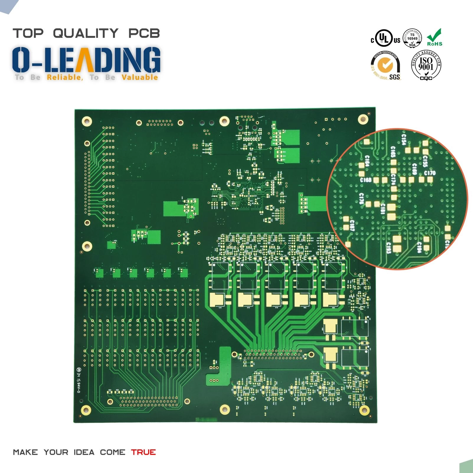
PCB design skills classic problem(二)
1. How to solve the contradiction between manual wiring and automatic wiring of high-speed signals?
At present, most of the automatic routers of strong routing software have set constraints to control the winding mode and the number of vias. The setting items of the winding engine capabilities and constraints of various EDA companies are sometimes quite different. For example, are there sufficient constraints to control the serpentine's meandering pattern, and to control the trace spacing of differential pairs? This will affect whether the auto-routed routing can meet the designer's idea. In addition, the difficulty of manually adjusting the wiring also has an absolute relationship with the ability of the winding engine. For example, the pushing ability of traces, the pushing ability of vias, and even the pushing ability of traces to copper plating. Therefore, choosing a router with a strong winding engine is the solution.
Lead free HAL wholesales china
2. About test coupons
The test coupon is used to measure whether the characteristic impedance of the produced PCB meets the design requirements by using TDR (Time Domain Reflectometer). Generally, the impedance to be controlled is a single wire and a differential pair. Therefore, the trace width and pitch (when there are differential pairs) on the test coupon should be the same as the lines to be controlled. The most important thing is the location of the ground point during the measurement. In order to reduce the inductance of the ground lead, the place where the TDR probe is grounded is usually very close to the probe tip. Therefore, the distance and method of the point where the signal is measured on the test coupon and the ground Match the probe used.
Lead free HASL wholesales china
3. In high-speed PCB design, the blank area of the signal layer can be copper-coated, and how should the copper-coating of multiple signal layers be allocated to ground and power?
Generally, the copper in the blank area is mostly grounded. Just pay attention to the distance between the copper and the signal line when laying copper next to the high-speed signal line, because the copper applied will reduce the characteristic impedance of the trace. Also be careful not to affect the characteristic impedance of its layers, such as in the structure of dual strip line.
