


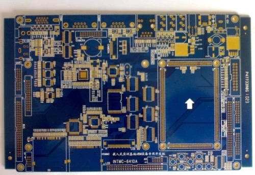
PCB signal integrity steps
o-leading
o-leading.com
2018-07-23 14:22:41
Before the design begins, you must think about and determine the design strategy to guide such things as component selection, process selection, and board production cost control.
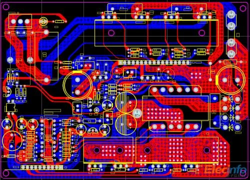
2. the cascading of the board
In the ideal case of complete signal, all high speed nodes should be routed within the impedance control inner layer (eg stripline). To optimize the SI and keep the board decoupled, the ground plane/power plane should be placed in pairs as much as possible. If you only have a pair of ground plane/power planes, you will only be there. If there is no power layer at all, you may encounter SI problems by definition. You may also encounter situations where it is difficult to simulate or simulate the performance of a board before the return path of the signal is defined.
3.crosstalk and impedance control
Coupling from adjacent signal lines will cause crosstalk and change the impedance of the signal lines. Coupling analysis of adjacent parallel signal lines may determine the "safe" or expected spacing (or parallel routing length) between signal lines or between various types of signal lines. For example, to limit the crosstalk of the clock to the data signal node to within 100mV, but to keep the signal traces parallel, you can find the minimum allowable spacing between the signals on any given wiring layer by calculation or simulation.(Printed circuit board manufacturer
)
4. important high-speed nodes
Delay and skew are key factors that must be considered for clock routing. Because of the tight timing requirements, such nodes typically must use termination devices to achieve the best SI quality. These nodes are pre-determined and the time required to adjust component placement and routing is planned to adjust the pointer for signal integrity design.
Different drive technologies are suitable for different tasks. Is the signal point-to-point or point-to-multiple? Is the signal output from the board or on the same board? What is the allowed time lag and noise margin? As a general guideline for signal integrity design, the slower the conversion speed, the better the signal integrity. A 2-3NS slew rate control device is fast enough to guarantee the quality of the SI and to help solve problems such as output synchronous switching (SSO) and electromagnetic compatibility (EMC).
6.pre-wired stage
The basic process of pre-wiring SI planning is to first define the input parameter range (drive amplitude, impedance, tracking speed) and possible topological range (min/max length, short line length, etc.), then run each possible simulation combination, analyze the timing and SI simulation results, finally find an acceptable range of values.
Next, the working range is interpreted as the wiring constraints of the PCB layout. This type of "cleaning" preparation can be performed using different software tools, and the routing program can automatically handle such wiring constraints. For most users, timing information is actually more important than SI results, and the results of the interconnect simulation can change the routing to adjust the timing of the signal path.
In other applications, this process can be used to determine the placement of pins or devices that are not compatible with system timing pointers. At this point, it is possible to completely determine the nodes that need to be manually routed or the nodes that do not need to be terminated. For programmable devices and ASICs, the choice of output driver can also be adjusted at this point to improve the SI design or avoid discrete termination devices.
7.SI simulation after wiring
In general, the SI design guidelines are difficult to ensure that no SI or timing issues occur after the actual cabling is completed. Even if the design is guided by the guide, unless you can continue to automatically check the design, there is no guarantee that the design will fully comply with the guidelines, so problems will inevitably occur. Post-wiring SI simulation checks will allow for planned breaks (or changes) in design rules, but this is only necessary for cost considerations or strict wiring requirements.(pcb board Printed company china)
Taking the above measures can ensure the SI design quality of the board. After the board assembly is completed, it is still necessary to place the board on the test platform, using an oscilloscope or TDR (time domain reflectometer) to measure the real board and simulation expectations. The results were compared. These measurements help you improve your model and manufacturing parameters so you can make better (less constraints) decisions in your next pre-design survey.
9.the choice of model
There are many articles on model selection, and engineers who have static timing verification may have noticed that although it is possible to obtain all the data from the device data table, it is still difficult to build a model. The SI simulation model is just the opposite. The model is easy to build, but the model data is difficult to obtain. Essentially, the only reliable source of SI model data is the IC supplier, who must maintain a tacit understanding with the design engineer. The IBIS model standard provides a consistent data carrier, but the establishment of the IBIS model and the guarantee of its quality are costly. IC suppliers still need market demand for this investment, and circuit board manufacturers may be the only demanders. market.