


Installation method of components on PCB printed circuit board
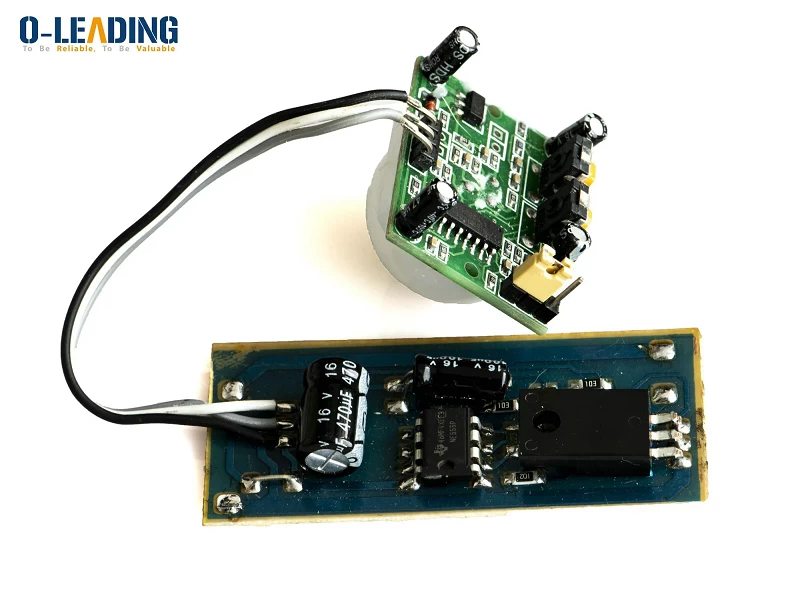
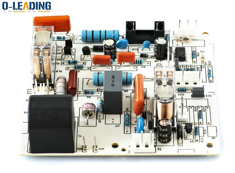
Our common computer board is basically epoxy resin glass cloth double-sided printed circuit board, one side of which is the inserted component and the other side is the component foot welding surface. We can see that the solder joints are very regular. We call it the pad for the discrete soldering surface of the component foot. Why not tin on other copper wire patterns? Because in addition to the pads and other parts that need to be soldered, the rest of the surface has a layer of wave soldering resistant solder mask. The surface of the solder mask is mostly green, and a few use yellow, black, blue, etc., so in the PCB industry, solder mask oil is often called green oil. Its function is to prevent bridging during wave soldering, improve soldering quality and save solder. It is also a permanent protective layer for printed boards, which can prevent moisture, corrosion, mildew and mechanical scratches. Viewed from the outside, the surface is smooth and bright green solder mask, which is the film that thermally cures green oil for the film. Not only does the appearance look better, but more importantly, its pad accuracy is higher, which improves the reliability of the solder joints.
FM Radio DIY Kit Electronic Production Kit pcba manufacturer
We can see from the computer board that there are three ways to install components. A plug-in installation process for transmission, which inserts electronic components into the through holes of the printed circuit board. In this way, it is easy to see that the through holes of the double-sided printed circuit board are as follows: one is the simple component insertion hole; the second is the component insertion and double-sided interconnection through hole; the third is the simple double-sided guide Through holes; fourth is the base plate installation and positioning holes. The other two mounting methods are surface mounting and chip direct mounting. In fact, the chip direct mounting technology can be regarded as a branch of surface mounting technology. It is to directly stick the chip to the printed board, and then use wire bonding or carrier tape method, flip chip method, beam lead method and other packaging technologies to interconnect to the printing. System board. The soldering surface is on the component surface.
Surface mounting technology has the following advantages:
1. Due to the large elimination of large vias or buried via interconnection technology on the printed board, the wiring density on the printed board is increased, the area of the printed board is reduced (generally one-third of the plug-in installation), and at the same time Can reduce the number of design layers and cost of printed boards.
2. Reduced weight, improved seismic performance, using gel solder and new soldering technology to improve product quality and reliability.
3. Due to the increased wiring density and shortened lead length, parasitic capacitance and parasitic inductance are reduced, which is more conducive to improving the electrical parameters of the printed board.
4. It is easier to automate than plug-in installation, improve the installation speed and labor productivity, and reduce the assembly cost accordingly.
Single side quick turn prototype pcba fabrication manufacturer
As can be seen from the above surface security technology, the improvement of circuit board technology is improved with the improvement of chip packaging technology and surface mounting technology. Now the computer board cards we see are constantly rising in surface sticking rate. In fact, this kind of circuit board reuse transmission screen printing circuit pattern can not meet the technical requirements. Therefore, the common high-precision circuit board, the circuit pattern and the solder mask pattern basically adopt the production process of photosensitive circuit and photosensitive green oil.
With the development trend of high-density circuit boards, the production requirements of circuit boards are getting higher and higher, and more and more new technologies are used in the production of circuit boards, such as laser technology, photosensitive resin and so on. The above is just a superficial introduction to some surfaces. There are many things in the production of circuit boards that are not explained due to space limitations, such as blind buried holes, winding boards, Teflon boards, lithography technology, etc.