


How to prevent PCB board deformation, several reasons are following:
When the PCB board is reflowed, it is easy to cause the board to bend. If it is serious, it will even cause the components to be welded, tombstone, etc. How to overcome it?
The damage of PCB board deformation:
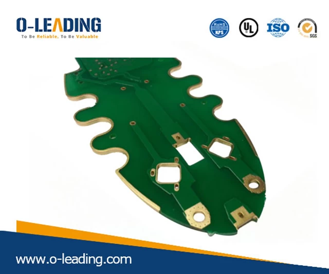
SMD stencil manufacturer china
On automated surface mount lines, if the board is not flat, it will cause misalignment, components can not be inserted or placed on the board's holes and surface mount pads, and even the automatic inserter will be damaged. The board on which the components are mounted is bent after soldering, and the component legs are difficult to trim. The board can't be installed in the chassis or the socket inside the machine, so it is very troublesome for the assembly factory to encounter the board. The current surface mount technology is moving toward high precision, high speed, and intelligent direction, which puts higher flatness requirements on PCB boards as homes for various components.
In the IPC standard, it is specifically pointed out that the maximum allowable deformation of a PCB board with a surface mount device is 0.75%, and the maximum allowable deformation of a PCB without a surface mount is 1.5%. In fact, in order to meet the needs of high-precision and high-speed placement, some electronic assembly manufacturers have stricter requirements on the amount of deformation. For example, the maximum deformation allowed by our company is 0.5%, and even individual customer requirements. 0.3%.
The PCB board is composed of copper foil, resin, glass cloth and other materials. The physical and chemical properties of each material are different. After pressing together, thermal stress remains inevitably, resulting in deformation. At the same time, in the processing of PCB, it will go through various processes such as high temperature, mechanical cutting and wet processing, which will also have an important impact on the deformation of the board. In short, the causes of PCB board deformation are complicated and diverse, how to reduce or eliminate the material characteristics. Different or processing-induced deformations have become one of the most complex problems faced by PCB manufacturers.
Analysis of the causes of PCB board deformation:
The deformation of PCB board needs to be studied from several aspects such as material, structure, pattern distribution, processing process, etc. This paper will analyze and expound various reasons and improvement methods that may cause deformation.
The uneven copper surface area on the board will deteriorate the board bend and the board curl.
Generally, a large area of copper foil is designed for grounding. Sometimes the Vcc layer is also designed with a large area of copper foil. When these large areas of copper foil are not evenly distributed on the same board. When it is on, it will cause the problem of uneven heat absorption and heat dissipation. The circuit board will of course also expand and contract. If the expansion and contraction cannot cause different stresses and deformation at the same time, the temperature of the board can be reached. At the upper end of the Tg value, the board begins to soften, causing permanent deformation.
The junctions (vias) of the various layers on the board limit the board's expansion and contraction.
Most of today's boards are multi-layer boards, and there are joints (vias) to the rivets between the layers. The joints are divided into through holes, blind holes and buried holes. Where there are joints, the board is limited. The effect of rising and contracting will indirectly cause the plate to bend and the plate to be warped.
Reasons for PCB board deformation:
(1) The weight of the circuit board itself will cause the board to be deformed
In general, the reflow furnace will use a chain to drive the advancement of the circuit board in the reflow furnace, that is, the two sides of the board are used as fulcrums to support the entire board. If the board has heavy parts on the board, or the size of the board is too large, It will show the phenomenon of the middle depression due to its own quantity, causing the plate to bend.
(2) The depth of the V-Cut and the connecting strip will affect the deformation of the panel.
Basically, V-Cut is the culprit in destroying the structure of the board. Because V-Cut cuts the groove on the original sheet, the V-Cut is prone to deformation.
2.1 Analysis of the deformation of the plate by pressing materials, structures and figures
The PCB board is formed by pressing a core board and a prepreg and an outer layer copper foil, wherein the core board and the copper foil are thermally deformed when pressed, and the amount of deformation depends on the coefficient of thermal expansion (CTE) of the two materials;
The coefficient of thermal expansion (CTE) of the copper foil is about 17×10-6;
The ordinary FR-4 substrate has a Z-direction CTE of (50-70) X10-6 at the Tg point;
Above TG point is (250~350) X10-6, X-direction CTE is similar to copper foil due to the presence of glass cloth.
Notes on TG points:
High Tg printed board When the temperature rises to a certain area, the substrate will change from "glass state" to "rubber state", and the temperature at this time is called the glass transition temperature (Tg) of the board. That is, Tg is the highest temperature (°C) at which the substrate remains rigid. That is to say, the ordinary PCB substrate material not only softens, deforms, melts, etc. at high temperatures, but also exhibits a sharp drop in mechanical and electrical properties.
Generally, the Tg plate is 130 degrees or more, the high Tg is generally greater than 170 degrees, and the medium Tg is greater than about 150 degrees.
A PCB printed board with a typical Tg ≥ 170 ° C is called a high Tg printed board.
The Tg of the substrate is improved, and the characteristics such as heat resistance, moisture resistance, chemical resistance, and stability of the printed board are improved and improved. The higher the TG value, the better the temperature resistance of the sheet, especially in the lead-free process, the high Tg application is more.
High Tg refers to high heat resistance. With the rapid development of the electronics industry, especially the electronic products represented by computers, the development of high functionality and high multi-layer requires the higher heat resistance of PCB substrate materials as an important guarantee. The emergence and development of high-density mounting technology represented by SMT and CMT makes PCBs more and more inseparable from the high heat resistance of substrates in terms of small aperture, fine wiring and thinning.