


How to improve the false welding phenomenon of soldering of circuit board
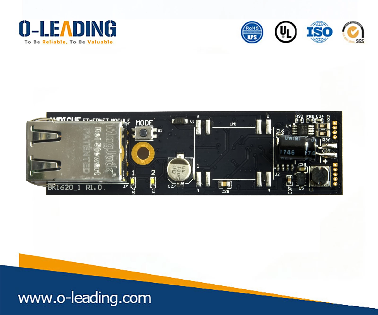
Net Power Module manufacturer china
1. Surface tension
The cohesion of tin-lead solder is even larger than that of water, making the solder a sphere to minimize its surface area (the same volume, the sphere has the smallest surface area compared to other geometries, to meet the minimum energy requirements) . The role of the flux is similar to the effect of the cleaning agent on the greased metal sheet. In addition, the surface tension is highly dependent on the cleanliness and temperature of the surface. The ideal stain can only occur if the adhesion energy is much greater than the surface energy (cohesion). tin.
2. Production of metal alloy complexes
The intermetallic bonds of copper and tin form grains, and the shape and size of the grains depend on the duration and strength of the temperature at the time of soldering. Less heat during welding can form a fine crystalline structure, resulting in an excellent solder joint with optimum strength. The processing time of the chip processing is too long, whether it is because the welding time is too long or because the temperature is too high or both, it will lead to a rough crystal structure, which is gravel and brittle, and the shear strength is small. .
3. Dip tin angle
When the temperature of the eutectic point of the solder is about 35 ° C higher, when a drop of solder is placed on the hot flux-coated surface, a meniscus is formed, and to some extent, the metal surface is tinned. It can be evaluated by the shape of the meniscus. If the solder meniscus has a distinct undercut, shaped like a water droplet on a greased metal plate, or even tends to be spherical, the metal is not solderable. Only the meniscus is stretched to a small angle of less than 30° to have good weldability.
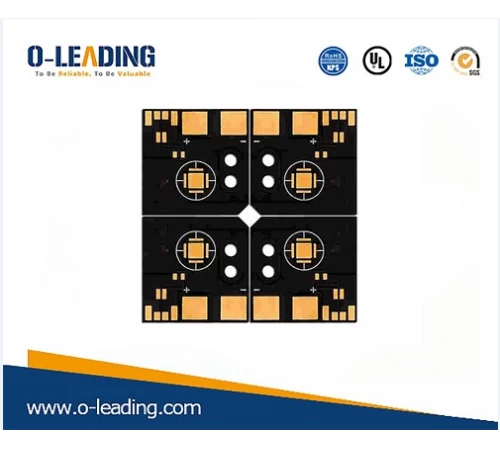
Immersion Gold manufacturer china
4. Dip tin effect
When hot liquid solder dissolves and penetrates the surface of the metal being welded, it is called metal tin or metal is tinned. The molecule of the mixture of solder and copper forms a new part of copper, which is a solder alloy. This solvent is called tin, which forms an intermolecular bond between the various parts to form a metal alloy complex. The formation of good intermolecular bonds is the core of the welding process, which determines the strength and quality of the solder joints. Only the surface of the copper is not contaminated, there is no oxide film formed by exposure to the air, and the solder and the working surface need to reach an appropriate temperature.
5. Copper is used as the metal substrate, tin-lead is used as the solder alloy, and lead and copper do not form any metal alloy complex. However, tin can penetrate into the copper, and the intermolecular bond between tin and copper is at the joint surface of the solder and the metal. Metal alloy alloys Cu3Sn and Cu6Sn5 are formed. The metal alloy layer (n phase + ε phase) must be very thin. In laser welding, the thickness of the metal alloy layer is 0.1 mm. In the wave soldering and manual soldering of PCB, the thickness of the intermetallic bond of the excellent solder joint is mostly exceeded. 0.5μm. Since the shear strength of the solder joint decreases as the thickness of the metal alloy layer increases, it is often tried to keep the thickness of the metal alloy layer below 1 μm, which can be achieved by making the soldering time as short as possible.Consigned PCB Assembly factory
The thickness of the metal alloy composite layer depends on the temperature and time at which the solder joint is formed. Ideally, the soldering should be completed within 220 't for about 2 seconds. Under this condition, the chemical diffusion reaction of copper and tin will produce an appropriate amount of metal. The alloy bonding materials Cu3Sn and Cu6Sn5 have a thickness of about 0.5 μm. Insufficient intermetallic bonds are common at cold solder joints or solder joints that are not raised to the proper temperature during soldering, which may result in the cutting of the soldered surface. Conversely, too thick a metal alloy layer, which is often used for solder joints that are overheated or soldered for too long, will result in very weak tensile strength at the solder joint.