


Resolves the problem that the PCB design impedance can not be continuous
Everyone knows that the impedance should be continuous. When PCB design always has an impedance that can not be continuous, what should I do?
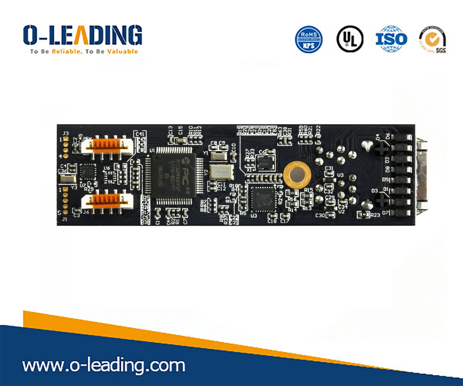
China double side PCB manufacturer
Characteristic impedance: also known as "characteristic impedance", it is not a direct current resistance and is a concept of long-range transmission. In the high-frequency field, during signal transmission, a signal is generated and an instantaneous current is generated between the signal line and the reference plane (power or ground plane) due to the electric field.
If the transmission line is isotropic, as long as the signal is in transmission, there is always a current I, and if the output voltage of the signal is V, during transmission of the signal, the transmission line is equivalent to a resistance, the size is V / I. This equivalent resistance is called the Z characteristic impedance of the transmission line.
During transmission of a signal, if the characteristic impedance of the transmission path changes, the signal will be reflected on the node where the impedance is discontinuous.
The factors influencing the characteristic impedance are: dielectric constant, dielectric thickness, line width and thickness of the copper sheet.
[1] Gradient line
Some RF devices have smaller packets, the widths of the SMD pad can be only 12 mils, and the widths of the RF signal can be more than 50 mils. A gradient line is used to disable abrupt changes to the line width. The gradient line is as shown in the figure, and the transition part line should not be too long.
[2] angle
If the RF signal line is at a right angle, the effective width of the line in the corner will increase and the impedance will be discontinuous, causing the reflection of the signal. To reduce discontinuities, there are two ways to handle corners: chamfers and fillets. The radius of the arc angle should be large enough. In general, it is guaranteed that R & gt; 3W. As shown on the right.
[3] Large pad
When there is a large pad on the 50 ohm microstrip line, the large pad is equivalent to the distributed capacity, which destroys the impedance continuity characteristic of the microstrip line. Two methods can be improved at the same time: first, the medium of the microstrip line is thickened, and therefore the ground plane below the pad is dug, which can reduce the distributed capacity of the pad. As shown below.[4] Way
A street is a metal cylinder that is plated outside the street between the upper and lower layers of the table. The signal paths connect the transmission lines on different levels. The via stub is the unused part of the street. The pads are ring-shaped pads that connect the cables to the upper or internal transmission lines. The isolation disk is an annular space in each power or ground plane to prevent short circuits to the power and ground planes.
Parasitic parameters of vias
After a rigorous analysis of the physical theory and approximation, the model of the equivalent loop circuit can be modeled as a series capacitor in series with each end of the inductor.

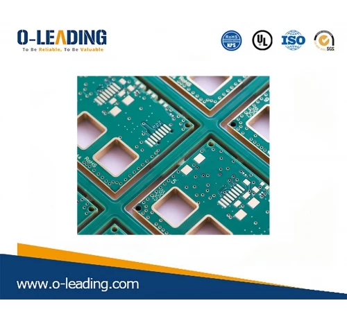
Professional multilayer PCB supplier
Passive circuit model
From the equivalent circuit model, the street hole itself has parasitic capacitance to the ground. Suppose that the diameter of the inverse pad is D2, that the pad diameter is D1, that the PCB board is T, and the dielectric constant of the board substrate is ε, the parasitic capacitance of the path is similar to:
The pathway parasitic capacitance can increase the signal rise time and the transmission speed slow down, thus degrading the signal quality. Likewise, the pathways also have parasitic inductance. In high-speed digital PCBs, parasitic inductance is often more harmful than parasitic capacitance.
Its parasitic series inductance weakens the contribution of the bypass capacitor, which reduces the filtering efficiency of the entire feeding system. Let L be the inductance of the way, h the length of the way, and d the diameter of the central hole. The parasitic inductance of the approximation via is approximate to:
Vias are one of the important factors that cause impedance discontinuity on the RF channel. If the signal frequency is above 1 GHz, consider the effects of Vias.
Common methods to reduce the impedance discontinuity are: using a diskless process, selecting the output mode, optimizing the antilock diameter and the like. Optimizing the diameter of the anti-bearing is one of the most common methods for reducing impedance discontinuities. Because the street characteristics are related to the dimensions of the structure such as the opening, the pad, the anti-pad, the stacked structure and the output mode, it is recommended that the HFSS and Optimizetrics are optimized for each project.
When using a parametric model, the modeling process is simple. At the time of review, the PCB designer is required to provide the corresponding simulation documentation.
The diameter of the way, the diameter of the bearing, the depth and the anti-bearing change, determine the impedance discontinuity, the reflection and the gravity of the insertion loss.
[5] Through coaxial connector
Similar to the street structure, the coaxial connector via also has impedance discontinuity, so the solution is the same as the street. A common method for reducing the impedance of the coaxial connector of the through hole is to use a diskless process, a suitable output mode and an optimized buffer diameter.