


PCB wiring guidelines
一. First, the board design steps
In general, the most basic process of designing a board can be divided into three major steps.
PCB Assembly manufacturer china
(1). Circuit schematic design: The circuit schematic design is mainly the PROTE099 schematic design system (Advanced Schematic) to draw a circuit schematic. In this process, we should make full use of the various schematic drawing tools and various editing functions provided by PROTEL99 to achieve our goal, that is, to obtain a correct and exquisite circuit schematic.
(2). Generate network table: The network table is a bridge between circuit schematic design (SCH) and printed circuit board design (PCB), which is the automatic soul of the circuit board. The netlist can be obtained from the schematic or extracted from the printed circuit board.
(3). Design of printed circuit board: The design of printed circuit board is mainly for PCB, another important part of PROTEL99. In this process, we use the powerful functions provided by PROTEL99 to realize the layout of the circuit board. , complete the difficult work and so on.
二. Second, draw a simple circuit diagram
Schematic Design Process The design of the schematic can be done as follows.
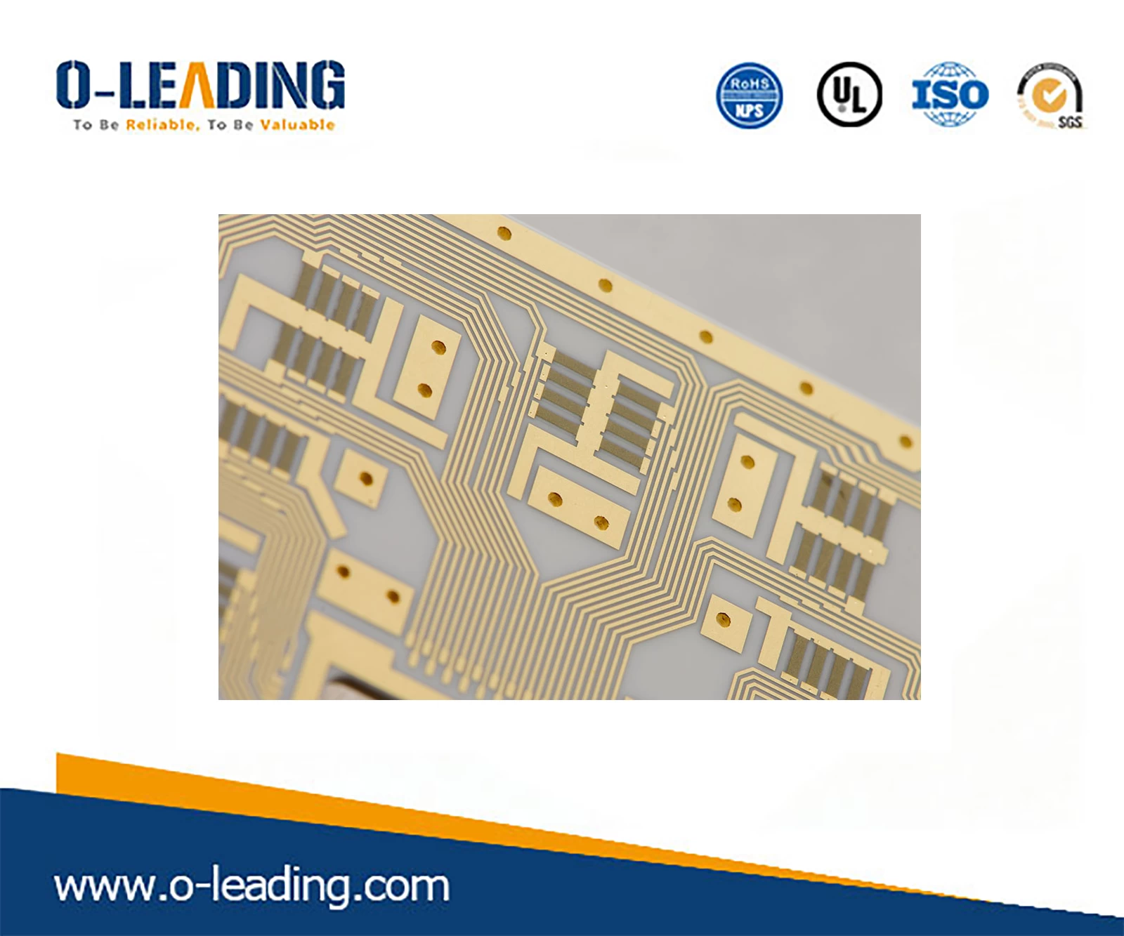
Ceramic Printed circuit board supplier
(1) Design drawing size After Protel 99/ Schematic, first plan the part drawing and design the drawing size. The size of the drawing is based on the size and complexity of the circuit diagram. Setting the appropriate drawing size is the first step in designing the schematic.
(2) Set Protel 99/Schematic design environment Set Protel 99/Schematic design environment, including setting grid size and type, cursor type, etc. Most parameters can also use system default values.
(3) Rotating parts According to the needs of the circuit diagram, the user takes out the parts from the parts library and places them on the drawing, and defines and sets the part number and part package of the placed parts.
(4) Schematic wiring With the various tools provided by Protel 99/Schematic, the components on the drawing are connected by electrically conductive wires and symbols to form a complete schematic.
(5) Adjusting the circuit The preliminary drawing of the circuit diagram is further adjusted and modified to make the schematic diagram more beautiful.
(6) Report output Various reports are generated by various reporting tools provided by Protel 99/Schematic. The most important report is the network table, which is prepared for subsequent board design through the network table.
(7) File saving and printout The final steps are file saving and printout.
The principles that must be followed in the design principles of the MCU control board are as follows:
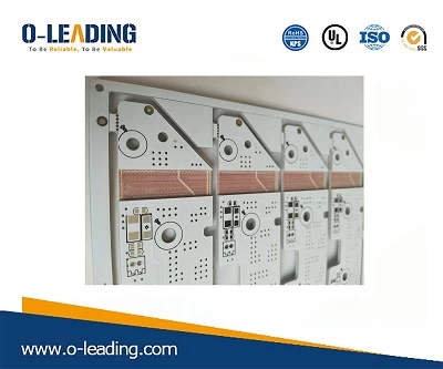
Multilayer pcb manufacturer china
三. In the layout of components, the related components should be placed as close as possible. For example, the clock generator, crystal oscillator, and CPU clock input are easy to generate noise. When placing them, they should be closer. . For those devices that are prone to noise, small current circuits, high-current circuit switching circuits, etc., try to keep them away from the logic control circuit and memory circuit (ROM, RAM) of the microcontroller, and if possible, make these circuits into circuits. The board is good for anti-interference and improves the reliability of the circuit.
(2) Try to install decoupling capacitors on the key components such as ROM, RAM and other chips. In fact, printed circuit board traces, pin connections, and wiring can all have large inductive effects. Large inductors can cause severe switching noise spikes on the Vcc trace. The only way to prevent switching noise spikes on the Vcc trace is to place a 0.1uF electronic decoupling capacitor between VCC and the power ground. If a surface mount component is used on the board, it can be mounted directly on the Vcc pin with a chip capacitor. It is best to use a ceramic capacitor because of its low electrostatic loss (ESL) and high frequency impedance, and the stability of the capacitor temperature and time is also good. Try not to use tantalum capacitors because of its high impedance at high frequencies. Pay attention to the following points when placing the decoupling capacitor:
Connect an electrolytic capacitor of about 100uF at the power input end of the printed circuit board. If the volume allows, the larger the capacitance, the better. In principle, a 0.01uF ceramic capacitor needs to be placed next to each integrated circuit chip. If the space of the circuit board is too small to be placed, a 1~10 tantalum capacitor can be placed around every 10 chips. For components with weak anti-interference ability, large current change during shutdown, and memory components such as RAM and ROM, a decoupling capacitor should be connected between the power supply line (Vcc) and the ground. The lead of the capacitor should not be too long, especially the high-frequency bypass capacitor can not be leaded.
(3) In the MCU control system, there are many types of ground wires, such as system ground, shield ground, logic ground, analog ground, etc. Whether the ground wire is properly laid out will determine the anti-interference ability of the circuit board. When designing ground and ground points, you should consider the following questions:
The logic ground and the analog ground are to be separately routed, and they cannot be used together, and their respective ground lines are respectively connected to the corresponding power ground lines. In the design, the analog ground wire should be as thick as possible, and the grounding area of the lead end should be increased as much as possible. Generally speaking, for the analog input and output signals, and the microcontroller