How do odd-numbered PCBs balance stacking and reduce costs?
Because of one less layer of dielectric and foil, the cost of raw materials for odd-numbered PCB is slightly lower than for even-numbered PCB. However, the processing cost of the odd-layer PCB is significantly higher than that of the even-layer PCB. The processing cost of the inner layer is the same; but the foil / core structure significantly increases the processing cost of the outer layer.
Odd-layer circuit boards need to add a non-standard laminated core-layer bonding process to the core structure process. Compared with the nuclear structure, the production efficiency of the factory in which the foil is added outside the nuclear structure will decrease. Before laminating and bonding, the outer core requires additional processing, which increases the risk of the outer layer being scratched and etched incorrectly.
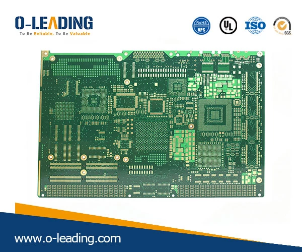
What if there are odd layers of PCBs in the design? The following methods can be used to achieve balanced stacking, reduce PCB manufacturing costs, and avoid PCB bending.
1) One signal layer and use. This method can be used if the power layer of the PCB is even and the signal layer is odd. Adding layers does not increase cost, but it can shorten delivery time and improve PCB quality.
4L Aluminum multilayer manufacturer china
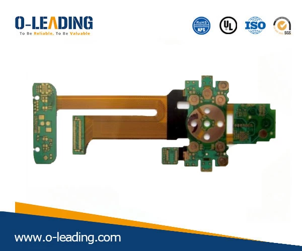
2) Add an additional power plane. This method can be used if the power layer of the PCB is odd and the signal layer is even. A simple method is to add a stratum in the middle of the stack without changing other settings. First route the PCBs according to the odd layers, then copy the ground layer in the middle and mark the remaining layers. This is the same as the electrical characteristics of a thickened layer of foil.
RoHs Compliant manufacturer china
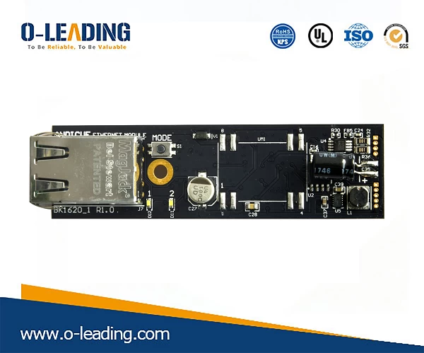
3)Add a blank signal layer near the center of the PCB stackup. This method minimizes stacking imbalances and improves PCB quality. Route the cables in odd layers first, then add a blank signal layer to mark the remaining layers. Used in microwave circuits and mixed dielectric (dielectrics with different dielectric constants) circuits.


