


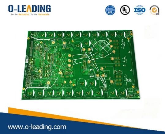
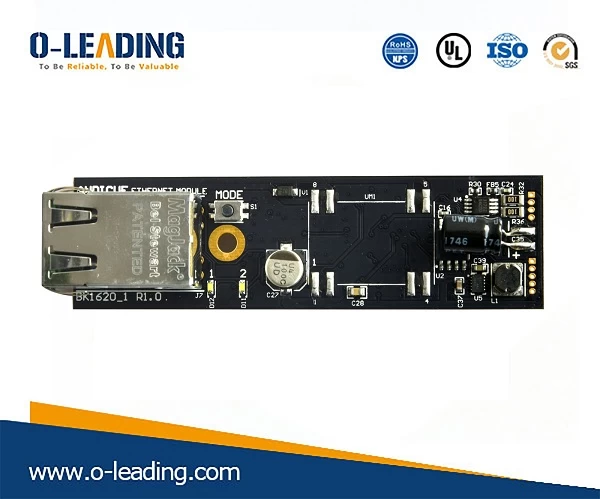
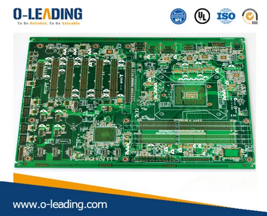
PCBA Process Introduction
PCBA, Printed Circuit Board Assembly, this is a technology mature industry, printed circuit board assembly; also called SMT, Surface Mounting Technology, surface mount technology. Those mounted components are called SMD, Surface Mounted Devices, and the process mainly refers to mounting electronic components on PCB printed circuit boards.
This article briefly introduces the typical process flow to give you a general understanding of the assembly of electronic products.
The first step is feeding: the PCB board is placed on the assembly line, with some automated loading racks, transmission belts, etc. Of course, before loading, there are also some pre-treatments on the PCB, such as baking, to eliminate internal stress.
The second step is to print the solder paste:
Screen-printed solder paste using a scraper and wire mesh. The technical difficulty is to control the printing accuracy and the thickness of the solder paste. The composition, viscosity, and stability of the solder paste are all important parameters. The printed solder paste has a little initial tack and can be bonded.
In addition to printing solder paste, some processes also print or dispense red glue, which is now relatively rare. Thermoset red glue is often used to reinforce components.
The third step is the patch:The patch is fully automatic and very fast. The red light is a visual positioning system. It can paste tens of thousands of capacitors and resistors per hour, but generally it is relatively small components such as capacitors and resistors.
For special-shaped or high-precision components, such as BGA and other chips, you need to use a universal machine, which will be slower. There are also medium speed machines, somewhere in between.
The fourth step: after the inspection is not abnormal, it is reflow after reflow, also called hot air leveling, tunnel furnace, etc.
The PCB with the components pasted is like a car going through a tunnel. Through a conveyor belt passing through the heating furnace above, the high temperature makes the solder paste flow easily, fully fills and wets the pads and components, and then cools down to form a reliable solder.
Step 5: Do the online test ICT, In Circuit Tester, use the probe to detect the line, or the AOI outside the line, use the image contrast to detect.
After bonding, there are still some large components that need to be inserted into the holes of the PCB board with pins. This is DIP, Dual In-line Package, and dual in-line package.
It can be operated by equipment or manual operation. After being inserted into the via hole on the PCB, it can be installed by manual soldering or wave soldering. Wave soldering is also a high-temperature process, which is a bit like reflow soldering, and it is easy for many people to confuse the two processes.
After the wave soldering is completed, the pins can be trimmed and then cleaned to remove some dirt residues caused during the process, such as FLUX solder resist. Then there is testing, packaging, and shipping.