


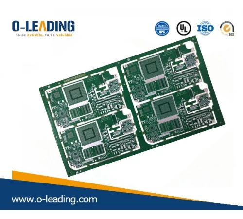
PCB board design analysis
First, the overlap of the pads

1. The overlap of the pads (except for the surface mount pads) means the overlap of the holes. In the drilling process, the drill bit is broken due to multiple holes in one hole, resulting in damage to the holes.
2. The two holes in the multi-layer board overlap, for example, one hole is the isolation plate, and the other hole is the connection plate (flower pad), so that the negative film is formed as a spacer disk, resulting in scrapping.
Second, the abuse of the graphics layer
1. Some useless connections were made on some graphics layers. Originally, four-layer boards were designed with more than five layers, which caused misunderstanding.
2, design time to save trouble, take Protel software as an example, the layers of each layer are drawn with the board layer, and the board layer is used to draw the line, so when the light drawing data is selected, because the board layer is not selected, it is missed. Wired and disconnected, or short-circuited by selecting the marking line of the Board layer, so the design layer is kept intact and clear.
3. Violation of the conventional design, such as the design of the component surface in the Bottom layer, the welding surface design in the Top, causing inconvenience.
Third, the random placement of characters
1. The character cover pad SMD soldering piece brings inconvenience to the on-off test of the printed board and the soldering of components.
2, the character design is too small, causing the difficulty of screen printing, too large will make the characters overlap each other, difficult to distinguish.
Fourth, the single-sided pad aperture setting
1. Single-sided pads are generally not drilled. If the holes are to be marked, the aperture should be designed to be zero. If a numerical value is designed, when the drilling data is generated, the coordinates of the hole appear at this position, and a problem occurs.
2. Single-sided pads such as drilled holes should be specially marked.
Fifth, draw pads with padding
Draw a pad with a pad to pass the DRC check when designing the line, but it is not suitable for processing. Therefore, the pad cannot directly generate solder resist data. When the solder resist is applied, the pad area will be covered by the solder resist, resulting in The device is difficult to solder.
Sixth, the electric ground layer is a flower pad and is a connection
Because the power is designed as a flower pad, the ground plane is the opposite of the image on the actual printed board, and all the connections are isolated lines, which should be very clear to the designer. By the way, when drawing several sets of power supplies or isolation lines of several grounds, care should be taken not to leave gaps, so that the two sets of power supplies are short-circuited, and the area of the connection cannot be blocked (so that a group of power supplies are separated).
Seven, the definition of processing level is not clear
1. The single-panel design is in the TOP layer. If you do not explain the positive and negative, the board may not be soldered.
2. For example, a four-layer board design uses four layers of TOPmid1 and mid2 bottom, but the processing is not performed in this order, which requires explanation.
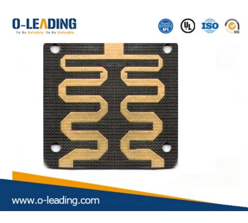
Blind-buried board supplier china
Eight, too many filler blocks in the design or filled blocks filled with very thin lines
1. The phenomenon that the light drawing data is lost is lost, and the light drawing data is not complete.
2. Because the filling block is drawn by lines one by one during the processing of the light drawing data, the amount of light drawing data generated is quite large, which increases the difficulty of data processing.
Nine, surface mount device pads are too short
This is for the on-off test. For a surface-mount device that is too dense, the spacing between the two legs is quite small, and the pads are also very thin. The test pins must be mounted up and down (left and right), such as pads. The design is too short, although it does not affect the device installation, it will make the test pin wrong.
Ten, the spacing of large area grid is too small
The edge between the large-area grid lines and the same line is too small (less than 0.3mm). During the manufacturing process of the printed board, the image transfer process is likely to cause a lot of broken film to adhere to the board after the completion of the shadow, resulting in disconnection.