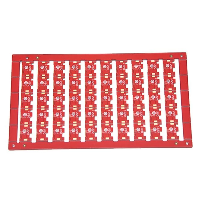
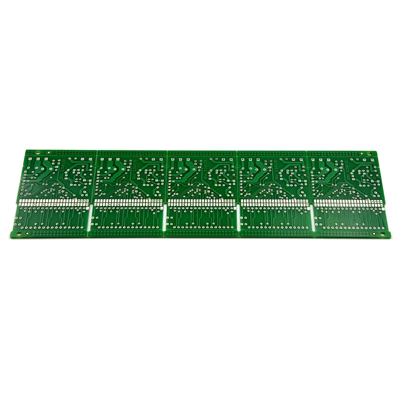
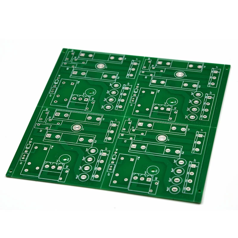
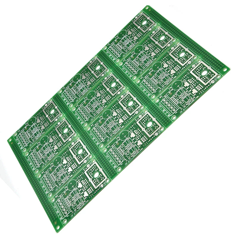
How is PCB producing a sample?
1 First of all, we need to tell the manufacturer the relevant data of the size, process requirements, quantity of products, etc. we need, and then there will be professional people to quote, order and follow up the production. CERAMIC WAFER manufacturer china
2 According to the requirements of the customer, cut the small piece of production board that meets the requirements on the sheet that meets the requirements. The specific process is as follows: large sheet material → cutting board according to MI requirements → board → round corner / edging → Come out.
flexible BOARD manufacturer china
3 The main operation is to drill according to the customer's data, and drill the size of the hole requested in the appropriate position. The specific process is as follows: stack pin → upper plate → drill hole → lower plate → inspection / repair.
4 The main operation is copper sinking. The principle of copper sinking is to deposit a thin layer of copper on the insulating hole by chemical method. The specific process is as follows: coarse grinding → hanging plate → copper sinking automatic line → lower plate → dip 1% diluted H2SO4 → Thicken copper.
5 This step is a graphics transfer, which refers to transferring the graphics on the production film to the large board. The specific process is as follows: Ma board → laminating → standing → aligning → exposure → standing → shooting → inspection.
Double Side PCB manufacturer china
6 Graphic plating is to deposit a layer of copper with the required thickness and a layer of gold or tin with the required thickness on the exposed copper skin or hole wall of the circuit pattern. The specific process is as follows: upper plate → degreasing → water washing twice → micro Etching → washing → pickling → copper plating → water washing → pickling → tin plating → water washing → lower plate.
7 This step is mainly to remove the anti-plating coating layer by using NaOH solution to expose the non-line copper layer.
8 etching process, the main operation is to use the chemical reagent copper to carry out the reaction, so that the non-line parts can be removed.
9 The process of green oil is to transfer the pattern of green oil film to the board. Its main function is to protect the line and prevent the tin on the line when welding the parts.
10 Mainly for printing some characters on the circuit board, the characters are mainly printed by some manufacturers' information and product information. The specific process is as follows: after the end of green oil → cooling and standing → adjusting the net → printing characters → after.
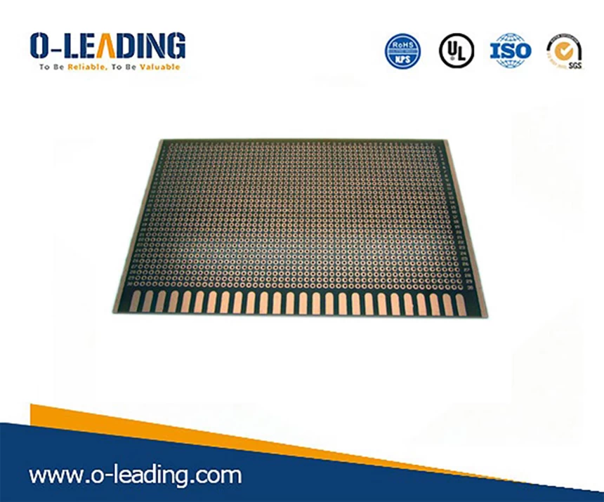
11 Gold-plated fingers: A layer of nickel/gold with a required thickness is applied to the fingers of the plug to make it more wear-resistant.
12 Molding: The method of shape molding required by the customer through the die stamping or numerical control machine is organic, beer, handcuffs and hand cut.
13 Circuit board test: It is mainly tested by flying probe tester to detect open circuit, short circuit and other defects that are not easily found on the circuit board.


