How UV lasers are used in the PCB industry
01
Is the CO2 laser or UV laser? Screen Printing Bending Ink wholesales.
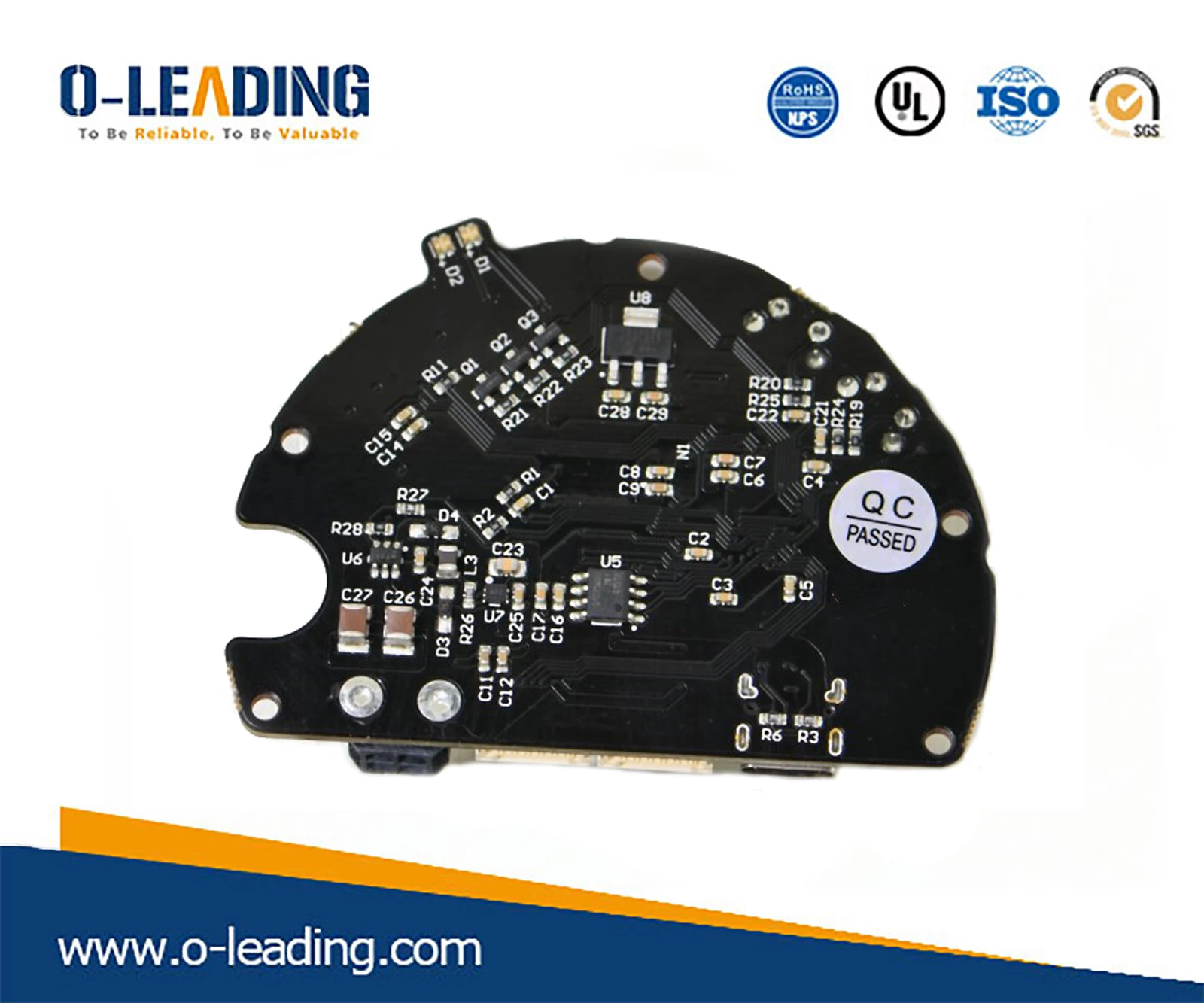
For example, when the PCB is divided or cut, a CO2 laser system with a wavelength of about 10.6 μm can be selected. However, it generates a lot of heat during the cutting process, causing severe carbonization of the edges. The UV laser has a wavelength of 355 nm. Laser beams of this wavelength are very easy to optically focus.
02
Advantages of UV laser processing
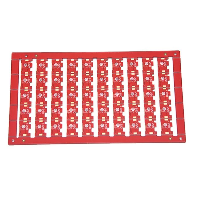
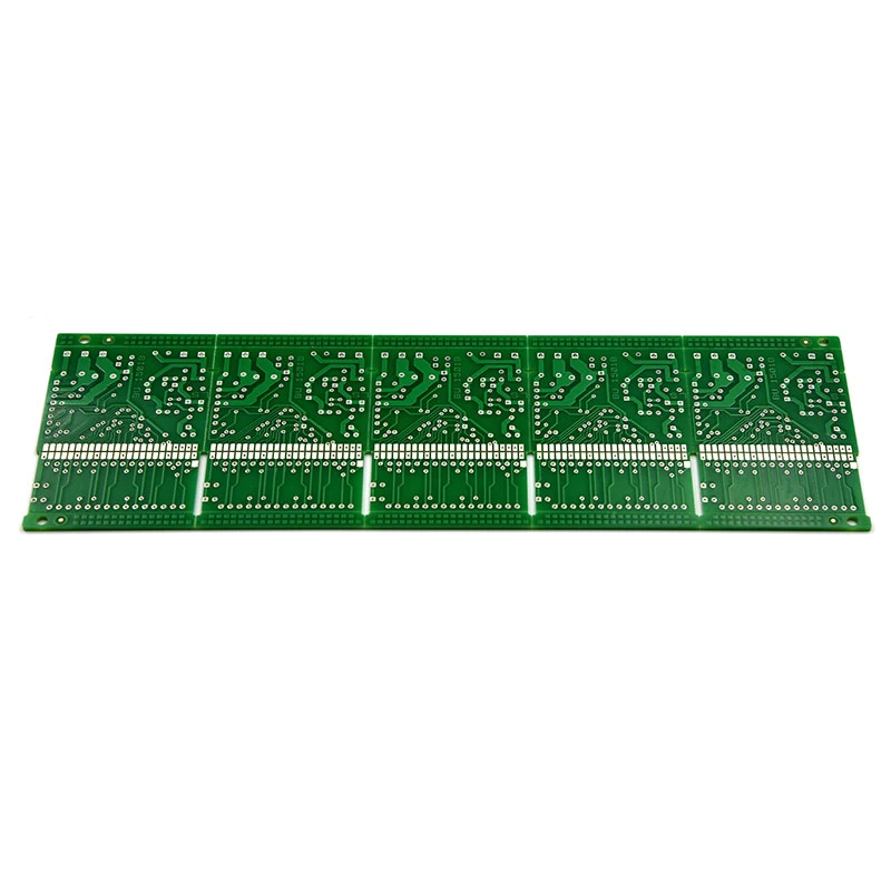
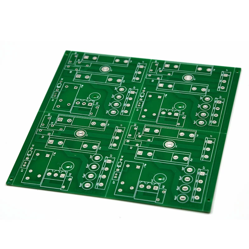
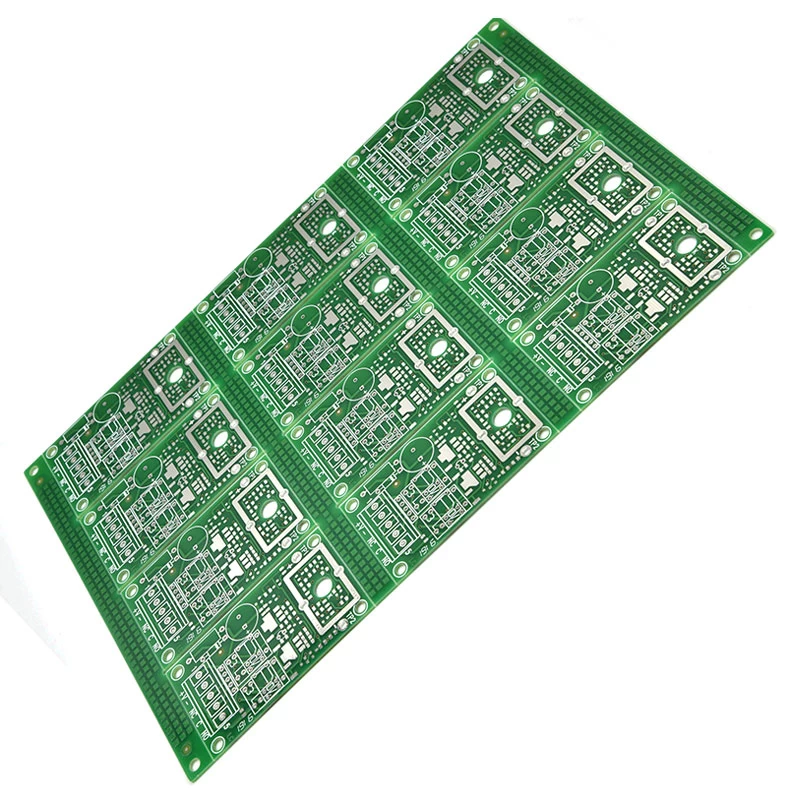
UV lasers are especially suitable for cutting and marking hard boards, soft and hard bonded boards, soft boards and their accessories.
UV laser cutting systems show great technical advantages. Depending on the thickness of the board material, the laser is cut one or more times along the desired profile. The thinner the material, the faster the cutting speed.
The pulse energy of the UV laser acts only on the material for a period of microseconds, and there is no significant thermal influence at the micrometers next to the slit, so there is no need to consider the damage caused by the heat generated by the component. The lines and solder joints near the edges are intact and burr-free.
GOLDEN FINGER BOARD supplier.
03
Drilling application
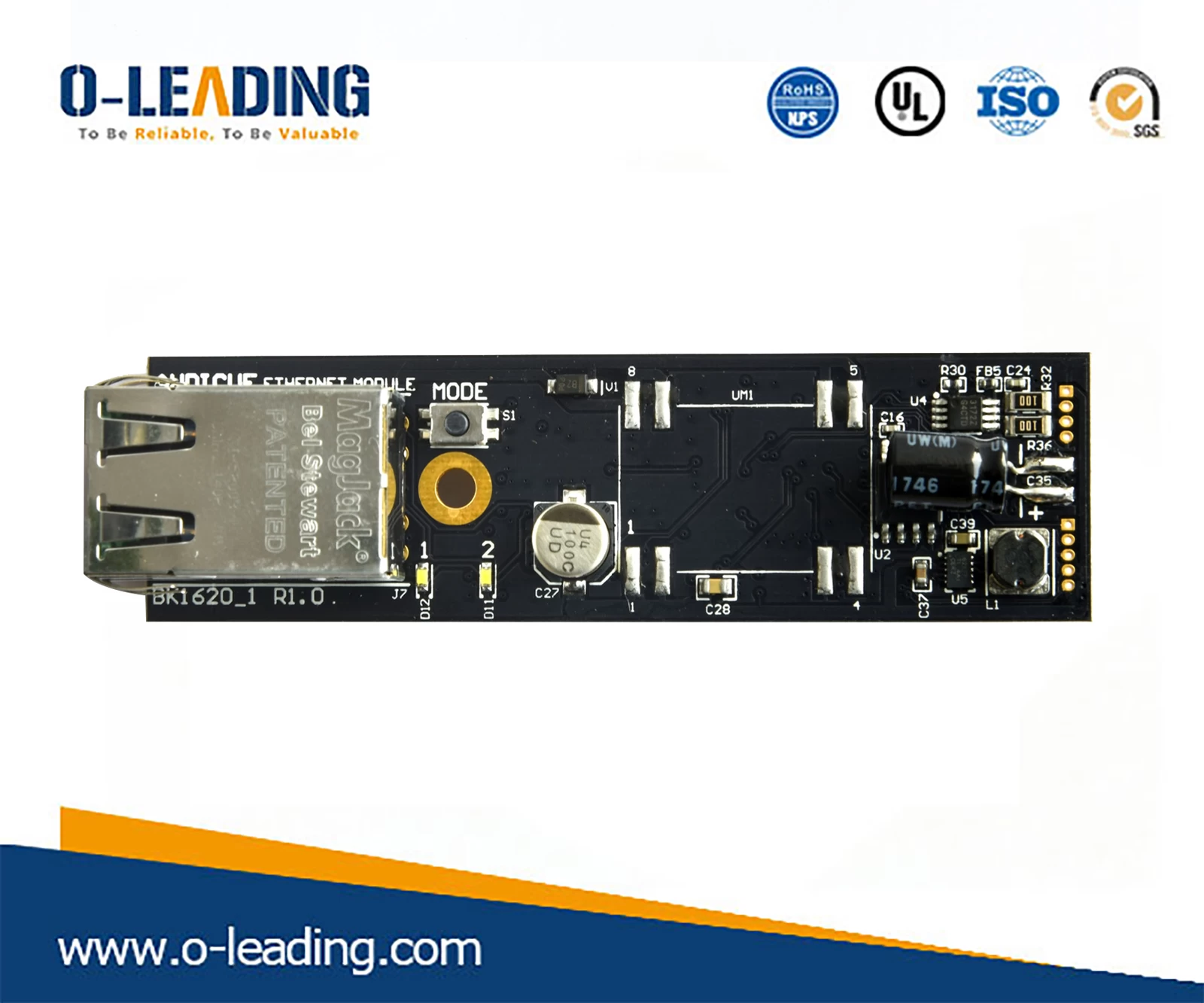
The through holes in the board are used to connect the front and back lines of the double panel or to connect any interlayer lines in the multilayer board. In order to conduct electricity, it is necessary to plate the hole walls with a metal layer after drilling. Nowadays, the traditional mechanical method can not meet the requirements of the smaller and smaller diameter of the drill hole: although the spindle speed is increased, the radial speed of the precision drilling tool will be reduced due to the small diameter, and even the required machining effect cannot be achieved. In addition, from an economic perspective, tool wear that is prone to wear is also a limiting factor.
04
Prepreg cutting
BACKPLANE BOARD manufacturer china.
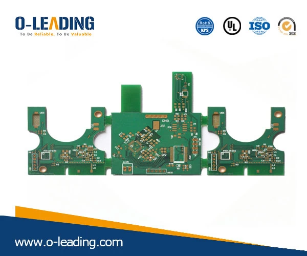
In the manufacturing process of electronic components, what conditions are required to cut the prepreg material? Early in the industry, prepreg materials have been used in multilayer boards. The various circuit layers in the multilayer circuit board are pressed together by the action of the prepreg; according to the circuit design, some areas of the prepreg need to be cut and opened before being pressed.
05
Soft and hard board processing
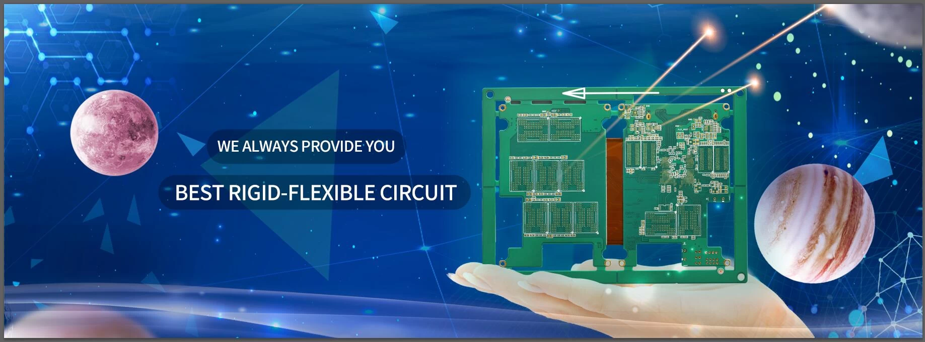
In the soft and hard bonding board, the rigid PCB is pressed together with the flexible PCB to form a multilayer board. During the pressing process, the flexible PCB is not pressed and bonded with the rigid PCB. The rigid cover covering the flexible PCB is cut and separated by laser deep cutting, leaving a flexible part to form a soft and hard bonding board.
Such deepening is also suitable for blind groove machining of surface-embedded integrated components in multilayer boards. The UV laser precisely cuts the blind grooves of the target layer separated from the multilayer board. In this region, the target layer is not connected to the material covered thereon.

