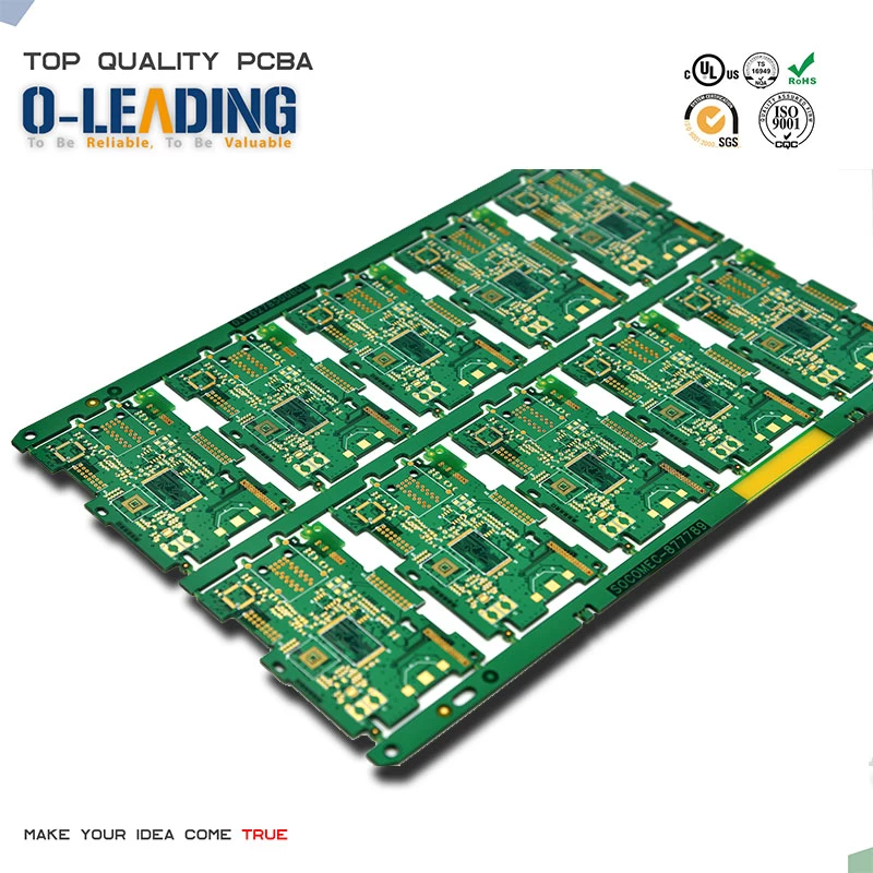
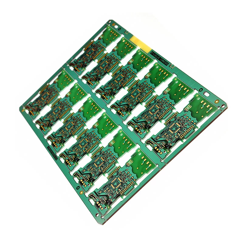
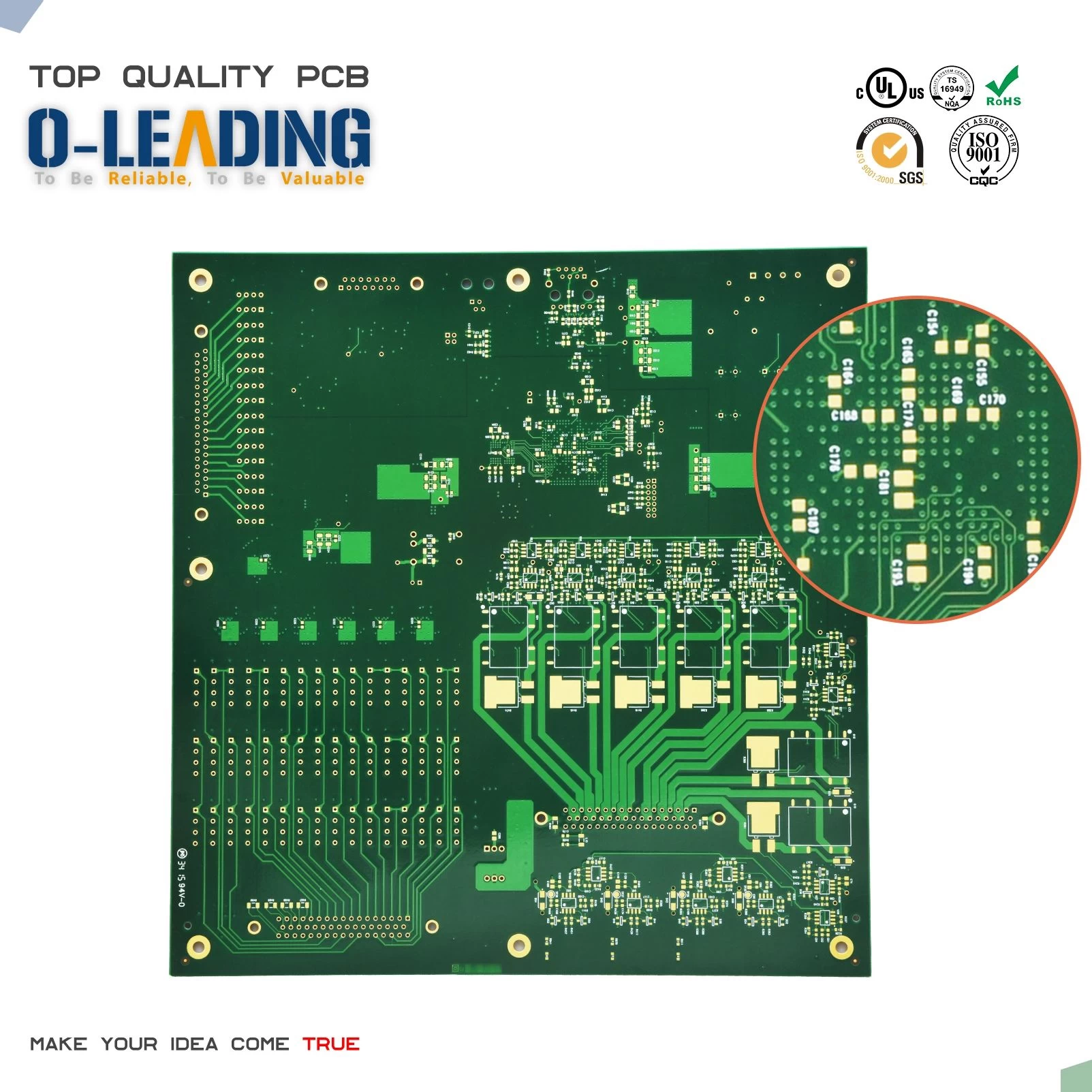
Do you know what the vias, blind holes, and buried holes of the PCB are?
Since this board is made by electronic printing, it is called a "printing" circuit board.LED Lighting manufacturer china.
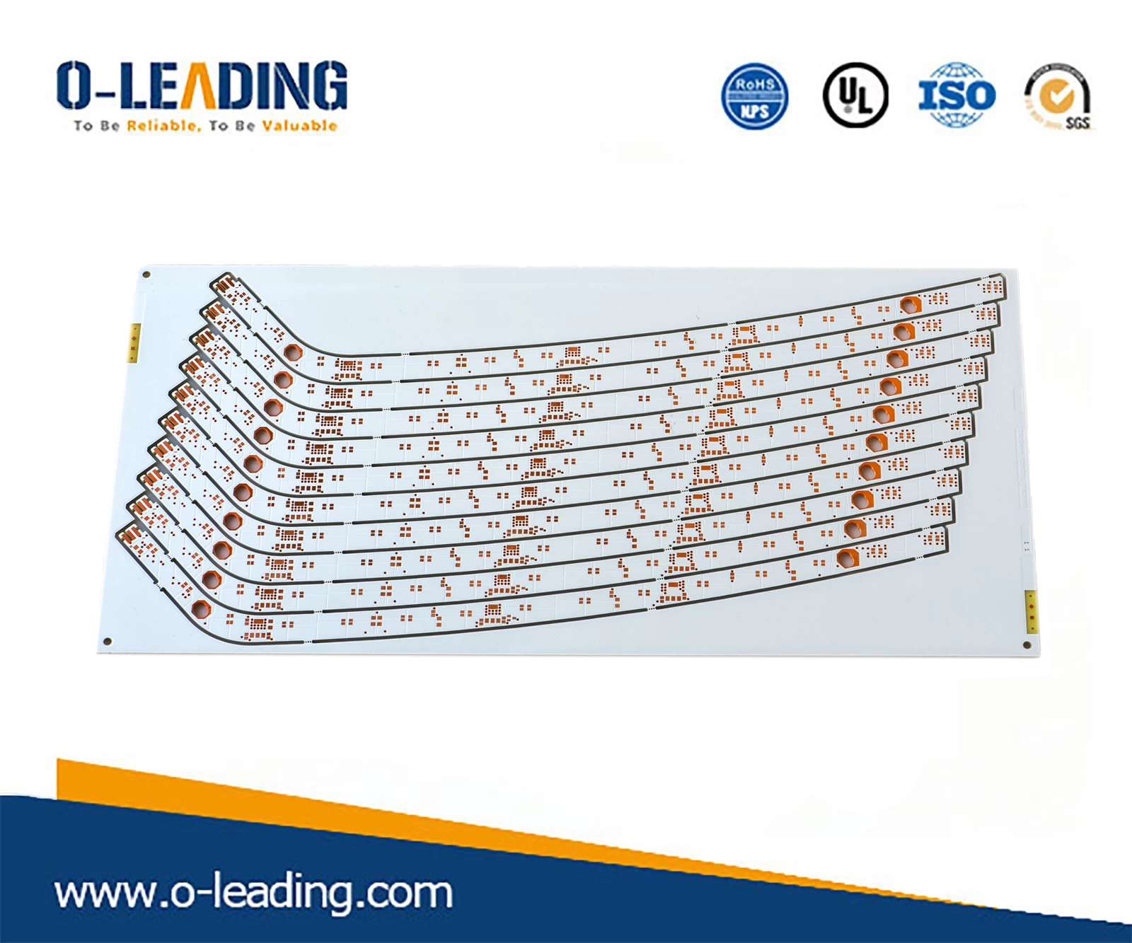
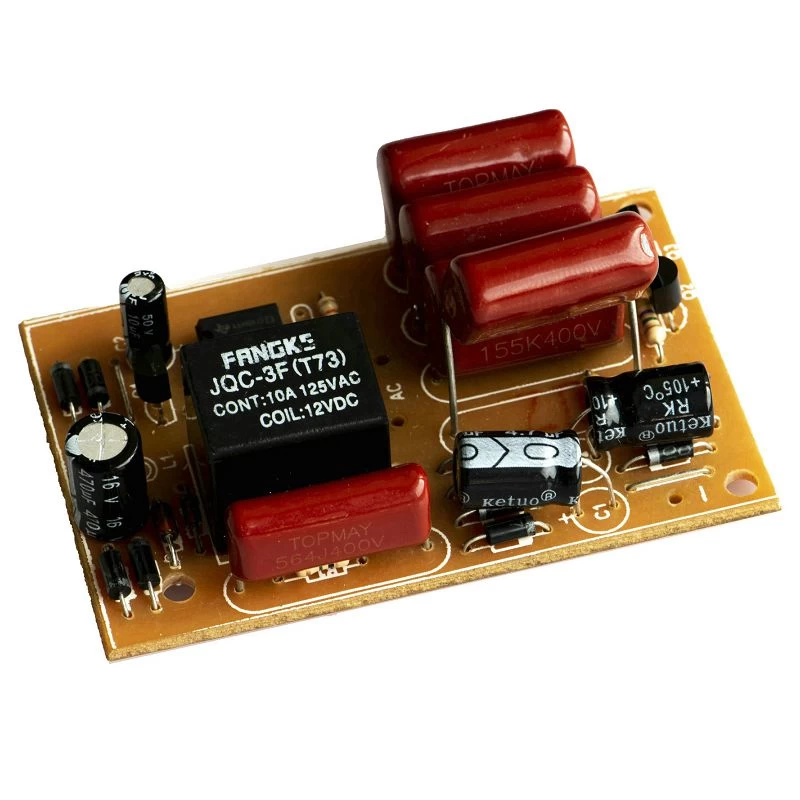
For the most basic PCB, the components are concentrated on one side, and the wires are concentrated on the other side. Because only one side can be wired, we call this PCB a single panel.
Single panel
Since only one side can be wired, sometimes it can't meet our requirements. All have double panels. Both sides of the double panel can be wired. Therefore, the wiring area is twice as large as that of the single panel, which is suitable for more complicated circuits.
Double panel
However, with the development of microelectronics technology, the complexity of the circuit has been greatly improved, and higher requirements have been placed on the electrical performance of the PCB. If a single panel or a double panel is also used, the circuit volume will be large, and the wiring will also be brought. A lot of difficulty, in addition, the electromagnetic interference between the lines is not easy to handle, so there are multi-layer boards (the number of layers represents several layers of independent wiring, usually even).EMBEDDED CAPACITANCE BOARD.
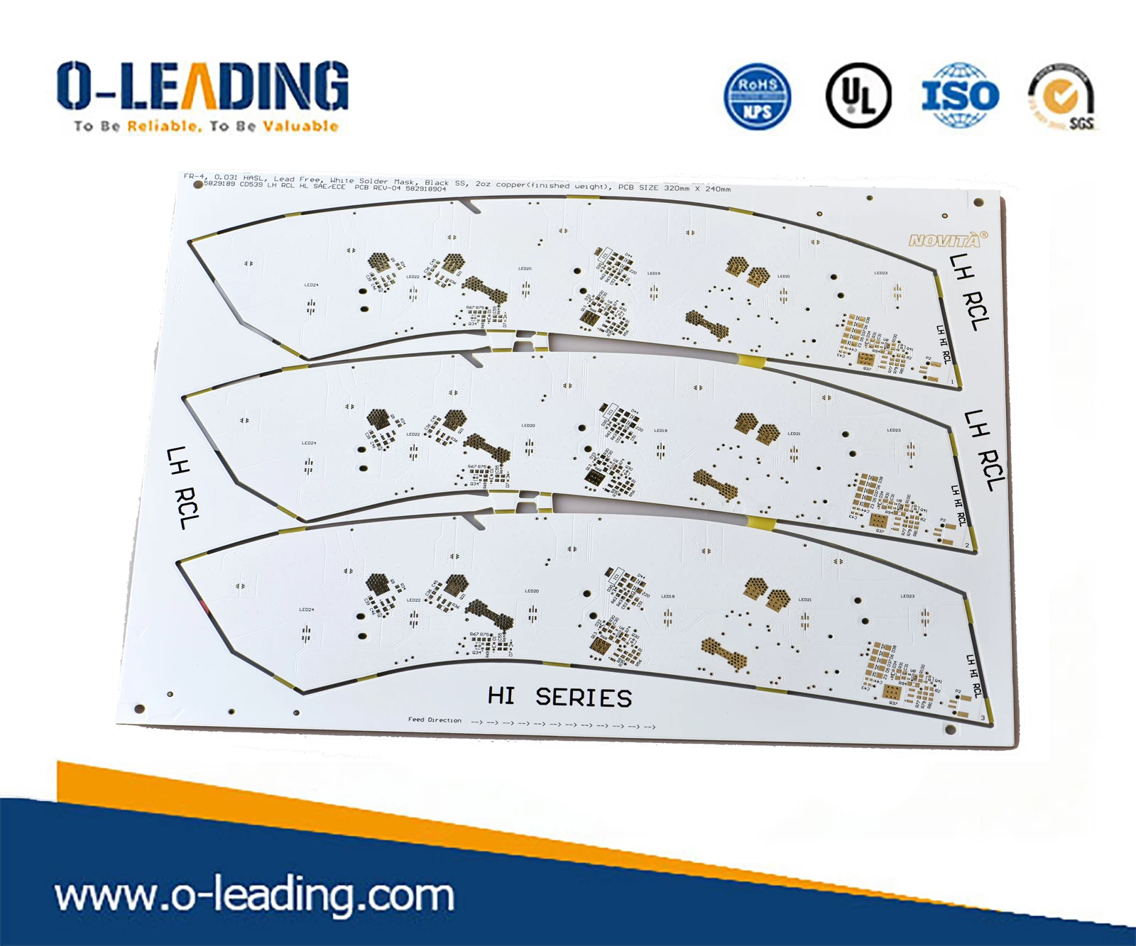
Multilayer boards are actually laminated and bonded by etched several single or double panels.
The multi-layer board has high assembly density and small volume; the connection between electronic components is shortened, the signal transmission speed is improved; the wiring is convenient; for the high-frequency circuit, the ground layer is added to make the signal line form a constant low impedance to the ground; The effect is good.
However, the higher the number of layers, the higher the cost, the longer the processing cycle, and the more troublesome quality inspection.
Our common computer boards usually use four or six layers.MICRO-WAVE MATERIAL HYBRID & ASSEMBLY BOARD.
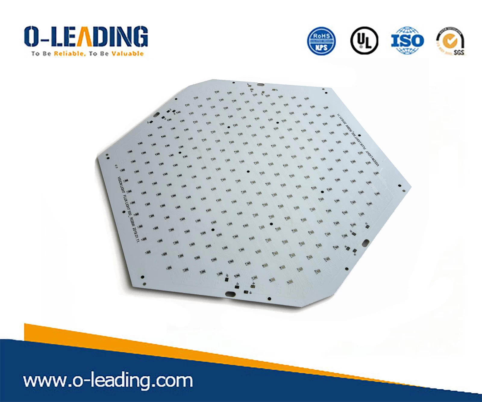
Multilayer board structure diagram
The biggest difference between PCB multi-layer boards and single-panel and double-panel is the addition of the internal power supply layer (maintaining the internal power layer) and the ground plane. The power and ground lines are mainly routed on the power plane. However, the multilayer wiring is mainly based on the top layer and the bottom layer, supplemented by the intermediate wiring layer.
Therefore, the design of the multi-layer board is basically the same as the design method of the double-sided board. The key point is how to optimize the wiring of the inner-layer, so that the wiring of the board is more reasonable and the electromagnetic compatibility is better.
In the double-panel and multi-layer boards, in order to connect the wires between the layers, a common hole, that is, a via hole, is drilled at the intersection of the wires that need to be connected at each layer.
Perforation structure diagram
In the process, the cylindrical surface of the hole wall of the via hole is chemically deposited with a layer of metal for connecting the copper foil to be connected in the middle layer, and the upper and lower sides of the via hole are formed into a circular pad shape. The via is different from the pad, and there is no solder layer on the via side.
A blind hole is a hole that starts from one surface and ends at the inner layer without penetrating the entire plate. That is, it can only be seen at one of the top or bottom layers, and the other layer is invisible.
Schematic diagram of blind hole and buried hole structure
A buried hole is a hole that does not pass through both outer surfaces and only penetrates in some inner layers. That is, the buried holes are buried inside the board, and these processes are not visible on the surface of the board.
In traditional PCB design, vias bring many problems. First, they take up a lot of effective space. Secondly, a large number of vias also cause huge obstacles to the inner layers of the multilayer PCB. These vias take up space for the traces. They densely pass through the surface of the power and ground planes, which can damage the impedance characteristics of the power ground plane.
The use of blind holes and buried holes can reduce the size of the PCB, improve electromagnetic compatibility, and make the design work easier and faster.
The disadvantages of using blind holes and buried holes are mainly the high cost of the board and the complicated processing, which increases the cost and the processing risk. It is not good to test and measure during debugging. Unless the board size is limited, it will be used when it is necessary.

