


Design irregular shape PCB
Today, PCBs are shrinking in size, and the functionality in boards is increasing, and as clock speeds increase, designs become more complex. So let's see how to handle more complex boards.
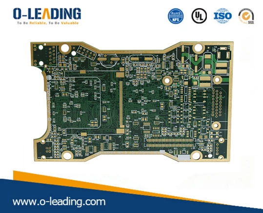
However, when the board shape needs to accommodate a complex housing with a high degree of limitation, it is not so easy for PCB designers because the functions in these tools are not the same as those of a mechanical CAD system. The complex circuit board shown in Figure 2 is mainly used for explosion-proof housings and is therefore subject to many mechanical limitations. Rebuilding this information in the EDA tool can take a long time and is not effective. Because it is very likely that mechanical engineers have created the enclosures, board shapes, mounting hole locations, and height limitations that PCB designers need.
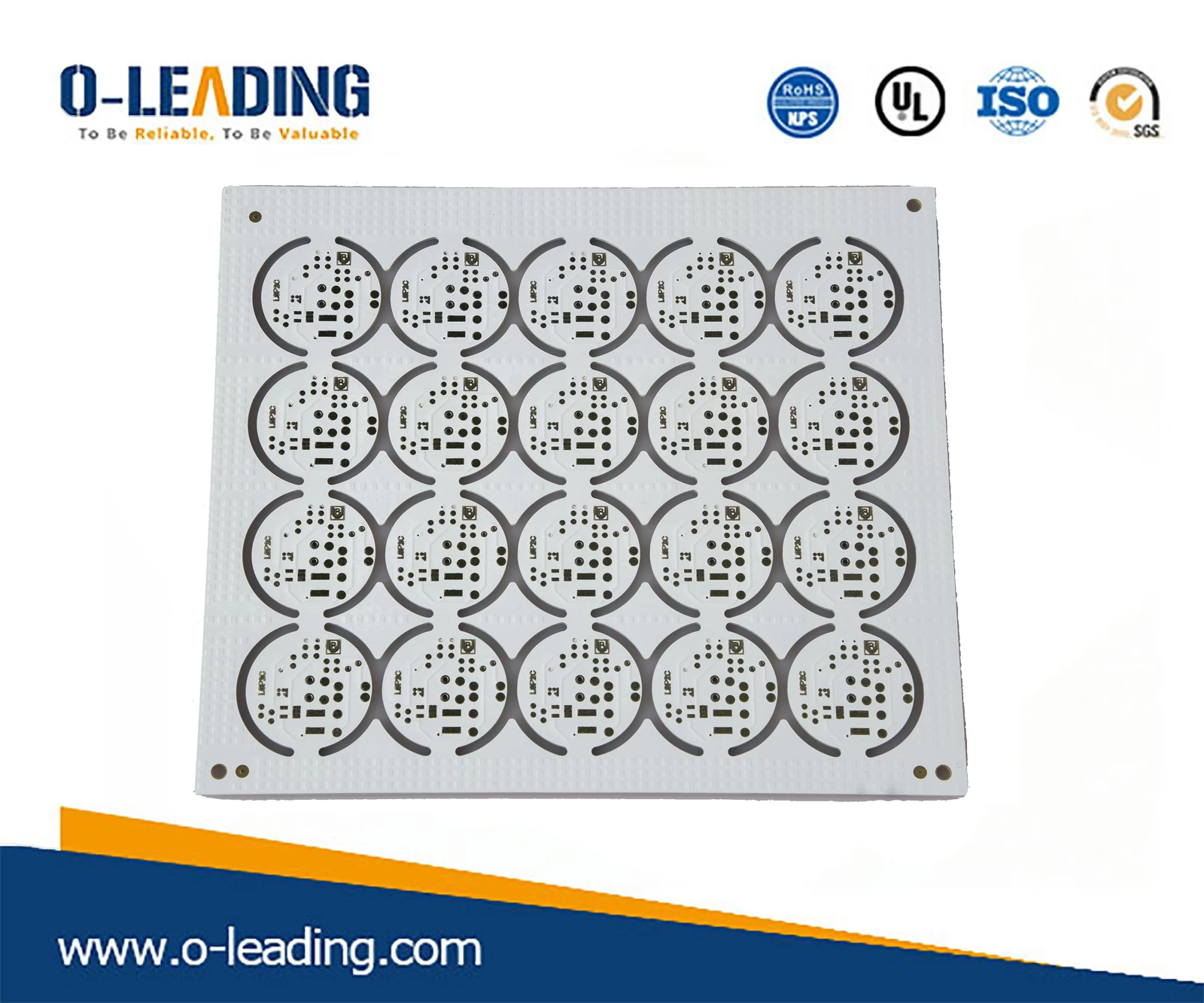
Because of the curvature and radius in the board, even if the board shape is not complicated (as shown in Figure 3), the reconstruction time may be longer than expected.
These are just a few examples of complex board shapes. However, from today's consumer electronics, you will be surprised to find that many projects attempt to include all the features in a small package that is not always rectangular. Your first thoughts should be on smartphones and tablets, but there are many similar examples.
So the question is “How do you import a defined mechanical engineering specification into a PCB design tool?” Reusing this data in a mechanical drawing eliminates duplication and, more importantly, eliminates human error.
We can solve this problem by importing all information into the PCB Layout software using the DXF, IDF or ProSTEP format. Doing so saves a lot of time and eliminates human error that can occur. Next, we will understand each of these formats one by one.