


What is the inside of the PCB?
High Density Interconnect Board (HDI)---via
The processing of the multilayer PCB is no different from the single-layer double layer. The biggest difference is in the process of via.
The lines are etched, and the vias are drilled and plated with copper.
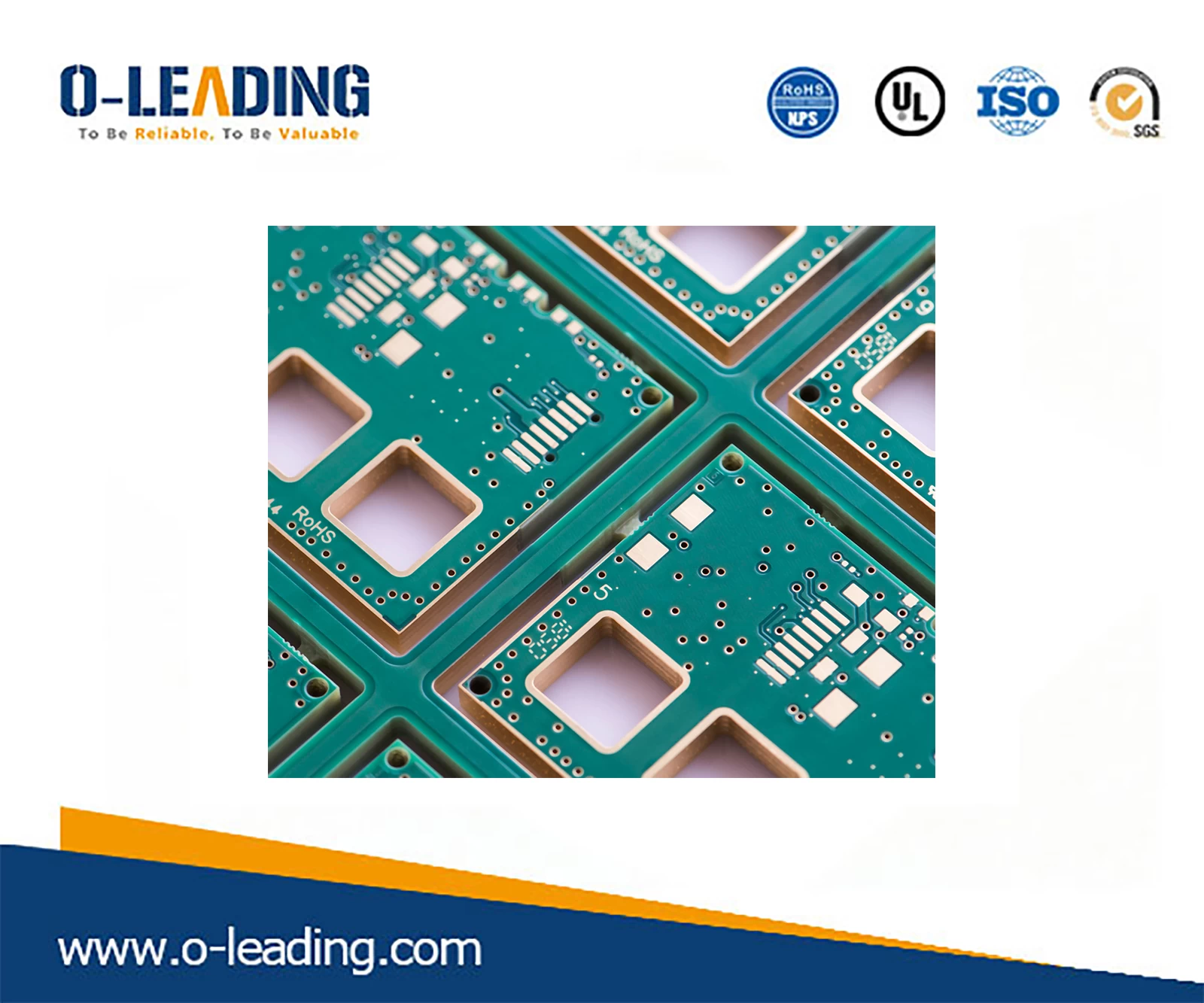
Multi-layer circuit boards usually have through-hole plates, first-order plates, second-order plates, and second-order stacked plates. Higher order, such as the third-order board, any layer of interconnection board is usually used very little, the price is expensive, not much discussion. FLEX BOARD supplier china.
Under normal circumstances, 8-bit MCU products use 2 layers of through-hole boards; 32-bit single-chip level intelligent hardware, using 4 layers and -6 layers of through-hole boards; Linux and Android-level intelligent hardware, using 6-layer through-hole to 8 first-order HDI board; a compact product such as a smart phone, generally uses an 8-layer first-order to 10-layer second-order circuit board.
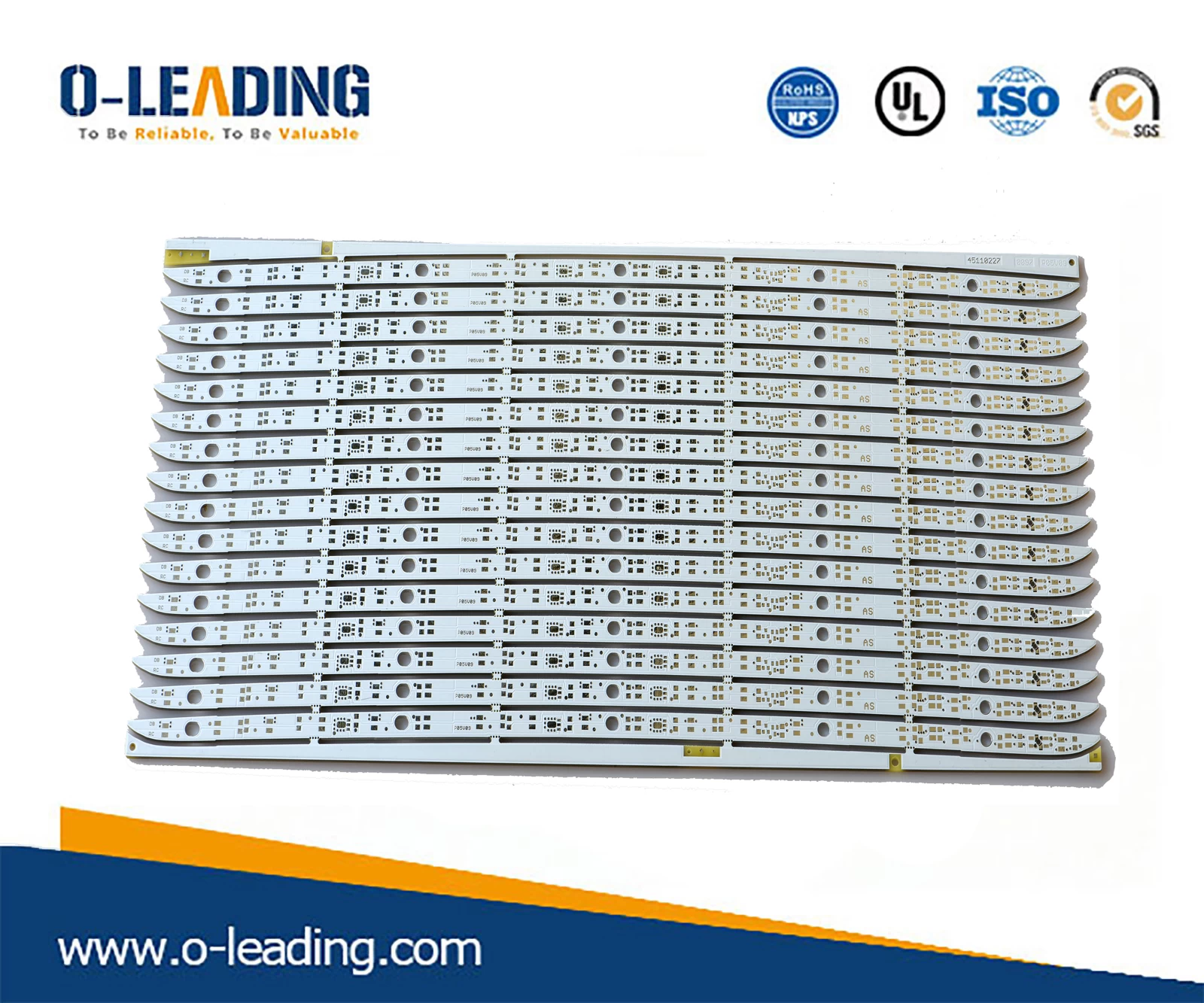
Most common through hole
There is only one type of via, from the first layer to the last layer. Whether it is an external line or an internal line, the holes are pierced. It is called a through hole plate.
flexible BOARD manufacturer china.
The number of through-hole plates and the number of layers does not matter. The two layers that are usually used by everyone are through-hole plates, and many switches and military circuit boards do 20 layers or through holes.
Drill the board through the drill bit and then plate the copper in the hole to form a path.
It should be noted here that the inner diameter of the through hole is usually 0.2 mm, 0.25 mm and 0.3 mm, but generally 0.2 mm is much more expensive than 0.3 mm. Because the drill bit is too thin and easy to break, the drill is also slower. The more time spent and the cost of the drill bit are reflected in the rise in board prices.
Double Side PCB manufacturer china.
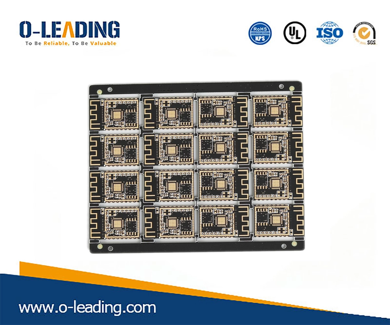
Laser hole for high density board (HDI board)
This picture is a laminated structure of a 6-layer 1st order HDI board. Both surfaces are laser holes and 0.1mm inner diameter. The inner layer is a mechanical hole
It is equivalent to a 4-layer through-hole plate and covers 2 layers on the outside.
The laser can only penetrate the fiberglass sheet and cannot penetrate the metal copper. Therefore, the punching of the outer surface does not affect other lines inside.
After the laser is punched, the copper is plated to form a laser via.
Super expensive any layer interconnect board, multi-layer laser stack
That is, each layer is a laser hole, and each layer can be connected together. I want to know how to drill the line and how to drill the hole.
Layout engineers think it feels cool! No longer afraid of painting!
If you want to cry, you want to cry. It is 10 times more expensive than ordinary through-hole plates!
Therefore, only products like the iPhone are willing to use. Other mobile phone brands have not heard of anyone who has used any layer of interconnected boards.