


PCB signal integrity design method
For PCB layout, signal integrity needs to provide a board layout that does not affect signal timing or voltage, while for circuit routing, signal integrity requires termination components, layout strategies, and routing information. High signal speeds on the PCB, incorrect layout of termination components, or incorrect wiring of high-speed signals can cause signal integrity problems, which can cause the system to output incorrect data, the circuit does not work properly, or does not work at all. How to fully consider the signal integrity factors in the PCB design process and take effective control measures has become a hot topic in the PCB design industry today.
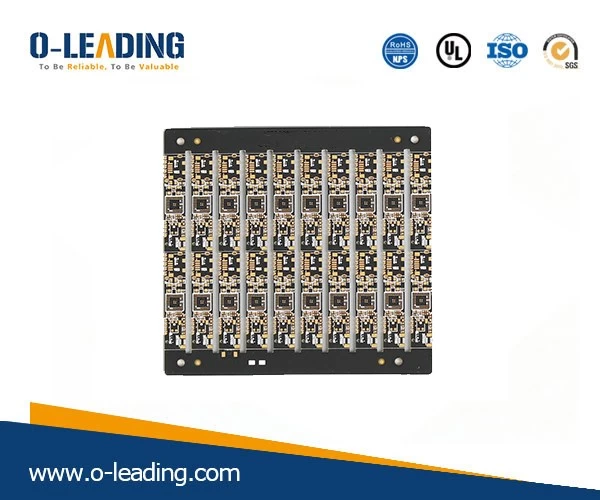
Multilayer pcb manufacturer china.
Signal integrity problem
Good signal integrity means that the signal responds with the correct timing and voltage level values when needed. Conversely, when the signal does not respond properly, a signal integrity problem occurs. Signal integrity issues can cause or directly introduce signal distortion, timing errors, incorrect data, address and control lines, and system malfunctions, even system crashes.
PCB signal integrity design method
In the practice of PCB design, people have accumulated a lot of design rules for circuit boards. In the PCB design, careful reference to these design rules can better achieve the signal integrity of the PCB.
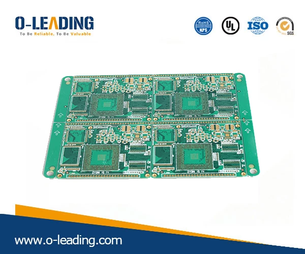
China Rigid-flexible pcb on sale.
When designing a PCB, you must first understand the design information of the entire board, which mainly includes:
1, the number of devices, device size, device package, chip rate, PCB is divided into low-speed medium-speed high-speed area, which is the interface input and output area;
2, the overall layout requirements, device layout location, the presence or absence of high-power devices, chip devices, heat dissipation special requirements;
3. Type and rate of signal lines, impedance control requirements of signal lines, bus speed trend and driving conditions, key signals and protection measures;
4, the type of power supply, the type of ground, noise tolerance requirements for power and ground, power supply and ground plane settings and segmentation;
5.The type and rate of the clock line, the source and destination of the clock line, the clock delay requirement, and the longest trace requirement.