


Six tips for choosing PCB components
1. Consider the choice of component package
During the schematic drawing phase, you should consider the component package and land pattern decisions you need to make during the layout phase. Some suggestions to consider when selecting components based on component packaging are given below.
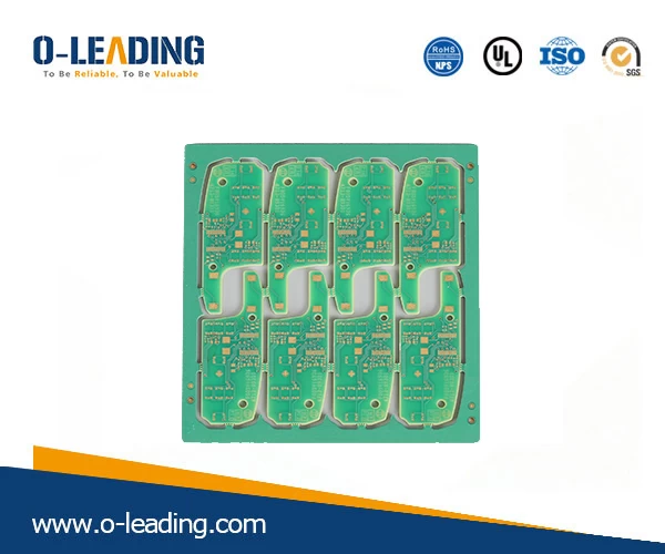
Halogen free pcb factory china.
• Remember that the package includes the electrical pad connections and mechanical dimensions (X, Y, and Z) of the component, ie the outline of the component body and the pins that connect the PCB. When selecting components, you need to consider any mounting or packaging restrictions that may exist on the top and bottom layers of the final PCB. Some components (such as polar capacitors) may have a high headroom limit that needs to be considered during the component selection process. When you first start designing, you can draw a basic board outline and then place some large or location-critical components (such as connectors) that you plan to use. In this way, the virtual perspective of the board (without wiring) can be seen intuitively and quickly, and the relative positioning and component height of the board and components are relatively accurate. This will help ensure that the assembled components of the PCB fit properly into the outer packaging (plastics, chassis, chassis, etc.). You can browse the entire board by calling 3D Preview mode from the Tools menu.
● The land pattern shows the actual pad or via shape of the soldered device on the PCB. These copper patterns on the PCB also contain some basic shape information. The size of the land pattern needs to be correct to ensure proper soldering and to ensure proper mechanical and thermal integrity of the connected components. When designing the PCB layout, you need to consider how the board will be manufactured, or how the pads will be soldered if soldered by hand. Reflow soldering (flux melting in a controlled high temperature furnace) can handle a wide range of surface mount devices (SMD). Wave soldering is typically used to solder the reverse side of a board to secure via devices, but it can also handle some surface mount components placed on the back side of the PCB. Typically, when using this technique, the underlying surface mount devices must be aligned in a particular direction, and in order to accommodate this soldering method, the pads may need to be modified.
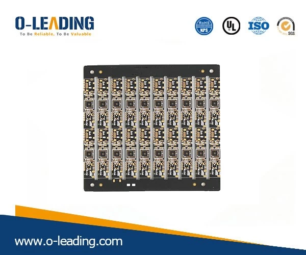
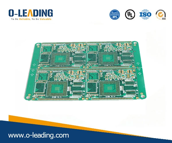
Multilayer PCB manufacturer in china.
● The choice of components can be changed throughout the design process. Early in the design process, it is determined which devices should use plated through holes (PTH) and which should use surface mount technology (SMT) to aid in the overall planning of the PCB. Factors to consider are device cost, availability, device area density, and power consumption. From a manufacturing perspective, surface mount devices are generally less expensive than through-hole devices and generally have higher availability. For small and medium-sized prototype projects, it is best to use larger surface mount devices or through-hole devices, which not only facilitates manual soldering, but also facilitates better connection pads and signals during troubleshooting and debugging.
● If there is no ready-made package in the database, it is common to create a custom package in the tool.
2. Use a good grounding method
Make sure the design has enough bypass capacitor and ground plane. When using an integrated circuit, be sure to use a suitable decoupling capacitor near the power supply to ground (preferably ground plane). The appropriate capacity of the capacitor depends on the specific application, capacitor technology and operating frequency. The electromagnetic compatibility and susceptibility of the circuit can be optimized when the bypass capacitor is placed between the power and ground pins and placed close to the correct IC pin.
3. Assign virtual component package
Print a bill of materials (BOM) to check the virtual components. Virtual components are not packaged and will not be transferred to the layout phase. Create a bill of materials and look at all the virtual components in the design. The only entries should be power and ground signals, because they are considered virtual components and are only processed in the schematic environment and are not passed to the layout design. Unless used for simulation purposes, components displayed in the virtual portion should be replaced with components with packages.
4. Make sure you have complete bill of materials data
Check the bill of materials report for sufficient complete data. After the bill of materials report has been created, a close inspection is performed to complete the incomplete device, supplier or manufacturer information in all component entries.
5. Sort by component label
To help sort and view the bill of materials, make sure the component labels are numbered consecutively.
6. Check the extra gates
In general, all redundant gate inputs should have a signal connection to prevent the input from floating. Make sure you check out any excess or missing gates and that all unwired inputs are fully connected. In some cases, if the input is in a floating state, the entire system will not work properly. Take the dual op amps that are often used in design. If only one of the op amps is used in a dual op amp IC component, it is recommended to either use the other op amp or ground the input of the unused op amp and place an appropriate unity gain (or other gain). The feedback network ensures that the entire component is working properly.
In some cases, ICs with floating pins may not work properly within the specification. Usually, the IC can only meet the specifications when the IC device or other gates in the same device are not operating in saturation. The input or output is close to or in the component supply rail. Simulations typically do not capture this situation because the simulation model typically does not connect multiple parts of the IC together to model the floating connection effect.