SMT solder paste printing process - steel mesh opening design guide
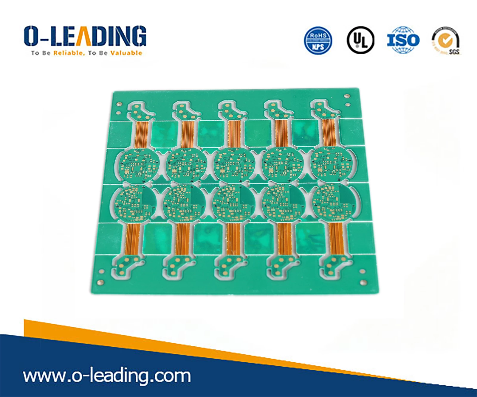
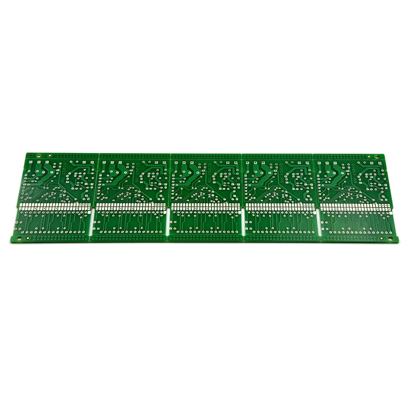
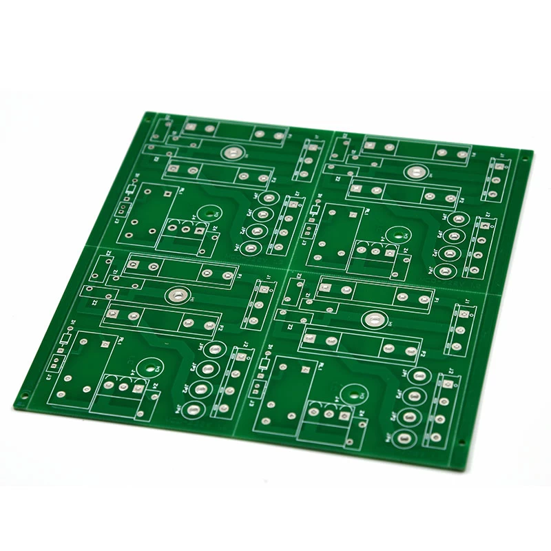
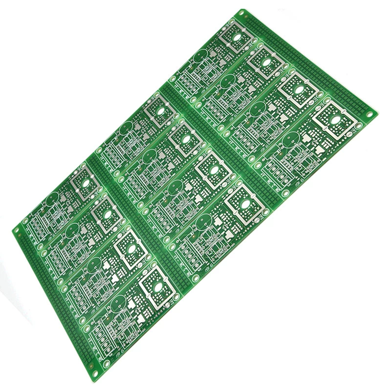
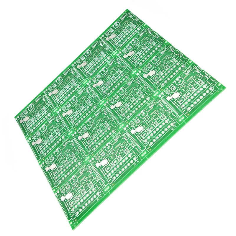
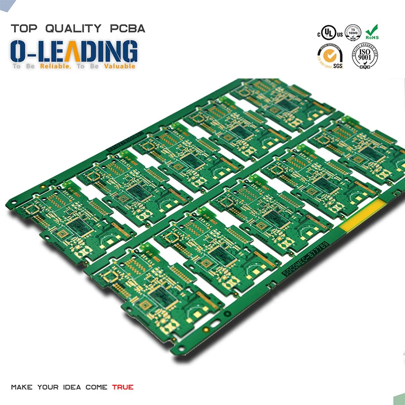
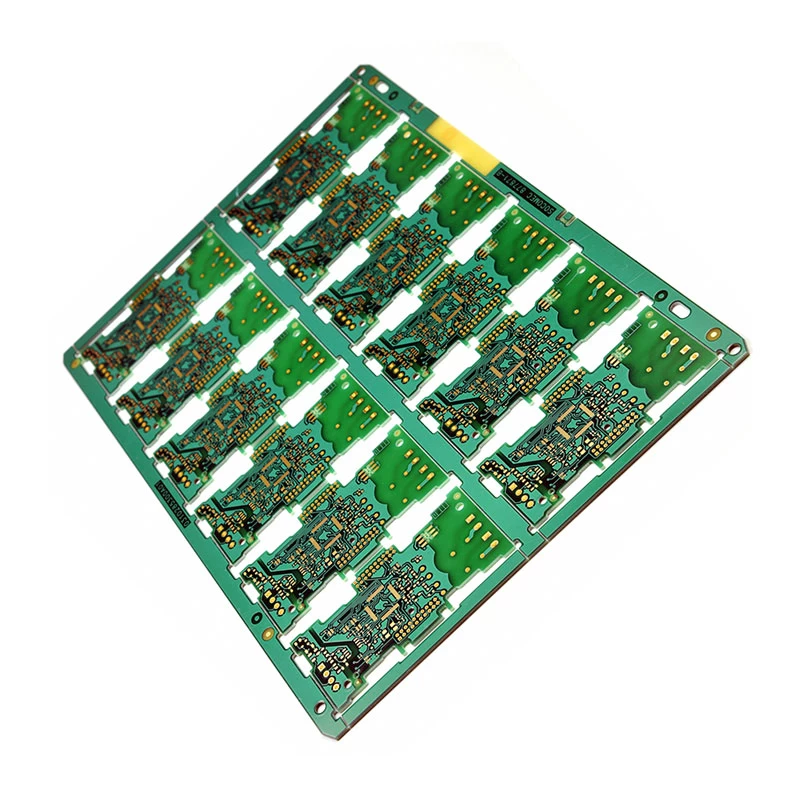
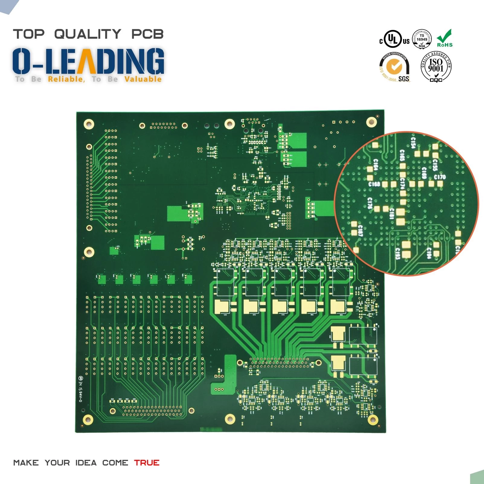
The thickness of the stencil and the size of the opening, the shape of the opening, the state of the inner wall of the opening, etc. determine the amount of solder paste printed, so the quality of the stencil directly affects the amount of solder paste printed PCB board. As SMT develops into high-density and ultra-high-density assemblies, stencil design becomes even more important.
Template thickness design
Stencil printing is contact printing, and the thickness of the stencil is a key parameter in determining the amount of solder paste.
The thickness of the stencil should be determined based on the printed board assembly density, component size, and spacing between pins (or solder balls).
Steel sheets having a thickness of 0.1 mm to 0.3 mm are usually used. For high-density assembly, a thickness of 0.1 mm or less can be selected.
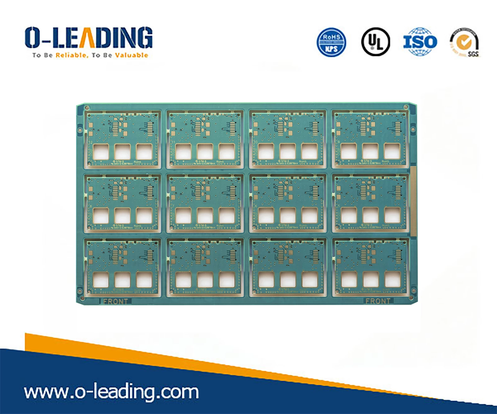
Generally, there are components with a general pitch of 1.27 mm or more on the same PCB, and narrow-pitch components. Components with a pitch of 1.27 mm or more need 0.2 mm thick, and components with narrow pitches need 0.15 to 0.1 mm thick. The thickness of the stainless steel plate can be determined according to the condition of most components on the PCB, and then the amount of the solder paste is adjusted by expanding or reducing the opening size of the individual component pads.
When the amount of solder paste is relatively large, the template at the narrow pitch component can be locally thinned.
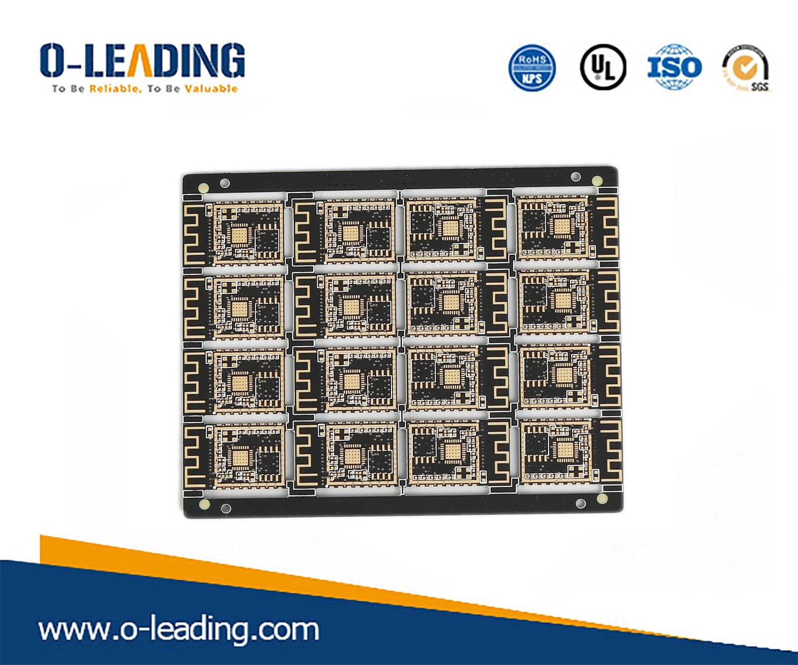
2. Template opening design
The template opening design contains two contents: opening size and opening shape PCB board.
Both the size of the mouth and the shape of the opening affect the filling and release of the solder paste (release film), which ultimately affects the amount of solder paste that is missing.
The template openings are designed according to the printed circuit board land pattern, and sometimes need to be modified (zoomed in, reduced or modified), because the amount of solder paste required for the structure, shape and size of the different component leads is different.
The larger the component size difference and the higher the assembly density on the same PCB, the more difficult the template design is.


