


PCB solderability design for PCBA manufacturability research
In view of the irrationality of such PCB soldering and solder mask design, the manufacturability and reliability problems, combined with the actual process level of PCB and PCBA, can be designed to avoid manufacturability problems through device package optimization. Optimization design mainly starts from two aspects, first, PCB LAYOUT optimization design; second, PCB engineering optimization design.
PCB LAYOUT design
Packages are packaged according to the IPC 7351 standard package and reference to the recommended pad size for the device specification. For fast design, Layout engineers prioritize the correction design according to the recommended pad size. The PCB solder pad design length and width are increased by 0.1mm. The solder mask is also based on the solder pad. Large 0.1mm.
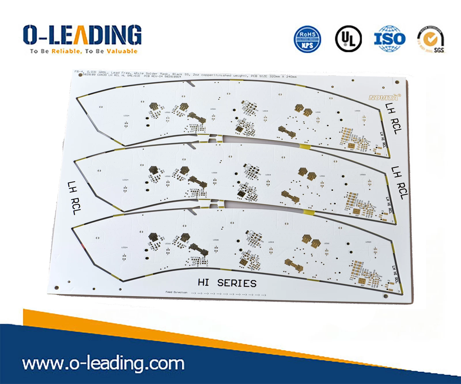
Golden Fingers PCB manufacturer china.

PCB LAYOUT design requirements
When the pads of the two soldering pad edges are more than 0.2mm apart, the package is designed according to the conventional pad; when the spacing of the two soldering pads is less than 0.2mm, the DFM optimization design and DFM optimization design are required. The method has optimized solder and solder pad size. When soldering the PCB, the solder mask in the solder mask process can form the minimum solder bridge isolation pad.
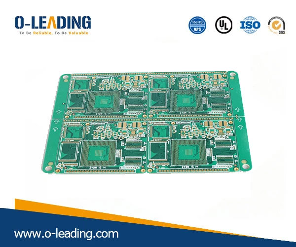
Multilayer PCB manufacturer china.
PCB engineering design requirements
When the pads with the edge spacing of the two soldering pads are more than 0.2mm, the engineering design is carried out according to the conventional requirements. When the spacing between the two pads is less than 0.2mm, the DFM design is required. The DFM method of the engineering design has the optimization and help of the solder mask design. Solder layer copper cutting; the copper size must refer to the device specification. The soldered pad after copper cutting should be within the recommended solder design size, and the PCB solder mask design should be a single pad window design, ie A solder mask can be covered between the pads. Ensure that there is a solder bridge in the middle of the PCBA during the PCBA manufacturing process to avoid the problem of solder appearance quality and electrical reliability.
Solder mask can effectively prevent solder bridging during soldering assembly. For high-density fine-pitch PCBs, PCBA processing plants cannot guarantee the local soldering quality if there is no solder bridge between them. For high-density fine pitch pins without soldering to isolate the PCB, the current PCBA manufacturing plant processing method is to determine the PCB material is not good, not on-line production. If the customer insists on going online, the PCBA manufacturing plant will not guarantee the quality of the welding in order to avoid the quality risk. It is predicted that the welding quality problems in the PCBA factory manufacturing process will be negotiated.