


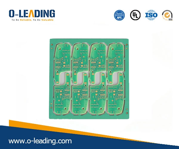
PCB process side design
When the PCB is to be subjected to SMT chip processing, the PCB is transported through the rails on the SMT line. Therefore, a pair of edges of the forbidden component must be left as the transfer side. Usually the two long sides of the PCB or the back of the panel are used as their transfer edges.
The width of the SMT transmission rail fixing plate is 3.0mm. In theory, the limit value of the conveying edge is 3.0mm, but it is recommended that you do not take this limit and increase the difficulty of the patch. To reserve more blanks as margin, it is recommended to use 5.0mm as the "prohibited area" for the transmitting side.
Halogen free pcb factory china
If the forbidden cloth is insufficient, after the PCB is transferred to the transfer rail, the interference part will affect the solder paste or the components already placed. The interference part of the board edge can only be post-welded or need another fixture to increase production. cost.
If the patch parts in the board are far enough away from the edge of the board and are not in the range of the track, there is no additional process side. If the part is in the track range, the process side must be added and the process side is used as the edge area. The width of the process side is usually 3-10mm depending on the machine characteristics, and 5mm is most common.
Multilayer pcb manufacturer china
Generally, the process is added to the longer side, and the board enters the SMT machine vertically, so that the hardness of the board is relatively high, and the patch does not bounce due to the light pressure of the machine probe, but the length of the process side is increased, and the disguise is increased. The average price of a single board. When the hardness of the board is sufficient, it can be added in a short direction, the area of the process side is small, the average cost of a single board is reduced, and the board is traversed into the SMT machine.
SMT usually uses MARK point to do the alignment. If there is no MARK point in the board, you must add 2-4 MARK points diagonally to the edge of the process. The size of the MARK point is generally 1.0mm, and the copper is on the tin. Next, the process side can be added or not.
Forming and testing are required for positioning during board production. Adding special positioning holes on the side of the process makes the shape relatively standard and it is convenient to make the positioning. Therefore, the process side will add 3-4 positioning holes between 2.0 and 4.0 mm in diameter, and the most common diameter is 3 mm, which is best used.