Line Width and Aperture Rule Settings Considerations
o-lead
o-leading.com
2018-05-22 14:11:55
Minimum line width/space 4mil
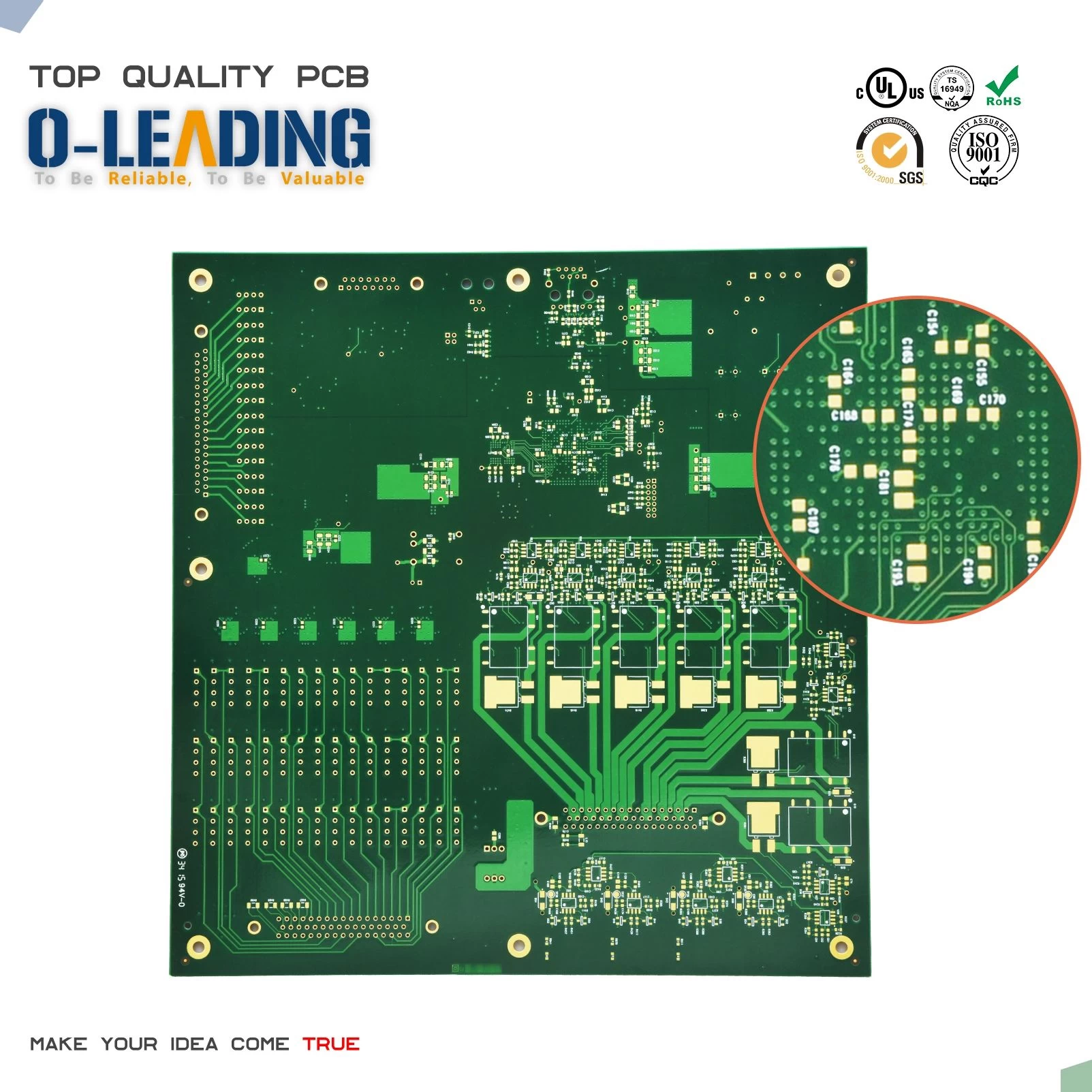
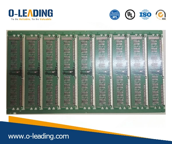
In PCB design, the highest precision that can be supported by batch processing is line width 4mil. That is, the width of the wiring must be greater than 4mil, and the spacing between the two lines also needs to be greater than 4mil. Of course, it is only the minimum limit of line width. In actual work, the line width needs to be defined as different values according to design requirements. For example, the definition of the power network is wider, and the definition of the signal line is more detailed. These different requirements can be defined in the rule Design - Rules - Routing - Width different line width values of different networks, and then according to the importance of setting rules to apply priority. Similarly, for line spacing, the electrical security spacing between different networks is defined in the rule page Design - Rules - Electrical - Clearance, and of course the line spacing.
There is also a special case. For high density pin components, the spacing between pads within the device is typically very small, such as 6 mils. Although meeting the minimum line width or manufacturing requirements with a pitch greater than 4 mils, it may not be suitable as a design PCB. Rule design requirements. If the minimum safety spacing setting for the entire PCB is 8 mils, then the pitch of component pads significantly violates the rule setting. When the rule is checked or edited online, it is always highlighted in green to show the violation. This kind of violation obviously does not need to be dealt with. We should correct the rule setting to eliminate green highlighting. In the original approach, separate security spacing rules for the device were defined using the query language and set to high priority. In the new version, only a simple check option is needed to solve this problem. Ignore Pad to Pad clearance within a footprint is ignored.
Checking with this option is very easy. You don't need to use the Query statement InComponent('U1') as it was, then set its minimum security spacing to 6mil and set it to the highest spacing priority.
Minimum mechanical aperture 0.2mm (8mil) Minimum laser aperture 4mil
Drill holes are inevitably used in PCB design. In terms of setting up the design rules and even the specific drilling operations, what kind of hole (through hole, blind hole, buried hole, or back hole?) and how many holes you drill should be drilled, you have a good idea. Yet? Will you be able to see how many holes are drilled by others and how many holes are drilled, or are you willing to fill in a size to meet the convenience of board layout and alignment?
The hole type is shown in the figure below. In general, less complicated designs, through-holes are often used in designs where there are not many plate stacks. In the complex design, especially the multilayer board, high speed and high density design, PCB wiring space requirements are very high, according to the actual need to set blind or buried holes. Of course, the blind buried hole is more complex than the through hole in the manufacturing process, and the manufacturing cost will increase accordingly.
The hole type is shown in the figure below. In general, less complicated designs, through-holes are often used in designs where there are not many plate stacks. In the complex design, especially the multilayer board, high speed and high density design, PCB wiring space requirements are very high, according to the actual need to set blind or buried holes. Of course, the blind buried hole is more complex than the through hole in the manufacturing process, and the manufacturing cost will increase accordingly.
If you want to see more interesting news like this, pleaese click the link: Custom Circuit Boards china.


