How to Realize the Anti-ESD Design of PCB?
o-leading.com
o-leading.com
2017-12-18 14:36:44
In the design of the PCB board, the anti-ESD design of the PCB can be realized through the layering, the proper layout, wiring and installation. Here are some common precautions:
1, use multi-layer PCB as much as possible
Compared to double-sided PCBs, the ground plane and power plane, as well as the closely spaced signal-to-ground spacing, reduce common mode impedance and inductive coupling to 1/10 to 1/100 of the double-sided PCB. Try to place each signal layer close to a power or ground plane. For components on both the top and bottom surfaces, with very short connections and many fill-in, high-density PCBs, Printed circuit board manufacturer could consider lining.
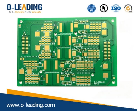
2, for double-sided PCB, to use closely intertwined power and ground grid.
Place the power cord close to the ground and connect as much as possible between the vertical and horizontal lines or fill area. The grid size on one side is 60 mm or less, and if possible, the grid size should be less than 13 mm.
3, to ensure that each circuit as compact as possible.
4, as far as possible all the connectors are aside. Printed circuit board in china
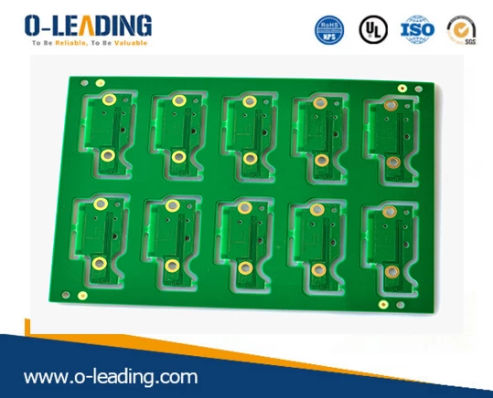 5, in each floor of the chassis and circuit ground, to set the same "isolation zone"; if possible, to maintain the separation distance of 0.64mm.
6, when the PCB assembly, do not apply any solder on the top or bottom pads.
Use screws with built-in washers to make the PCB come into close contact with the metal chassis / shield or the bracket on the ground plane.
7. If possible, introduce the power cord from the center of the card and away from areas prone to ESD.
8. Place the mounting holes on the edges of the card with the top and bottom pads of the solderless solder around the mounting holes to the chassis ground.
1, use multi-layer PCB as much as possible
Compared to double-sided PCBs, the ground plane and power plane, as well as the closely spaced signal-to-ground spacing, reduce common mode impedance and inductive coupling to 1/10 to 1/100 of the double-sided PCB. Try to place each signal layer close to a power or ground plane. For components on both the top and bottom surfaces, with very short connections and many fill-in, high-density PCBs, Printed circuit board manufacturer could consider lining.

2, for double-sided PCB, to use closely intertwined power and ground grid.
Place the power cord close to the ground and connect as much as possible between the vertical and horizontal lines or fill area. The grid size on one side is 60 mm or less, and if possible, the grid size should be less than 13 mm.
3, to ensure that each circuit as compact as possible.
4, as far as possible all the connectors are aside. Printed circuit board in china

6, when the PCB assembly, do not apply any solder on the top or bottom pads.
Use screws with built-in washers to make the PCB come into close contact with the metal chassis / shield or the bracket on the ground plane.
7. If possible, introduce the power cord from the center of the card and away from areas prone to ESD.
8. Place the mounting holes on the edges of the card with the top and bottom pads of the solderless solder around the mounting holes to the chassis ground.
Thanks for reading, for more information, you can click led pcb board Printed circuit board


