Capabilities: Laser-Drilled Micro-Vias
HDI and Micro-Vias
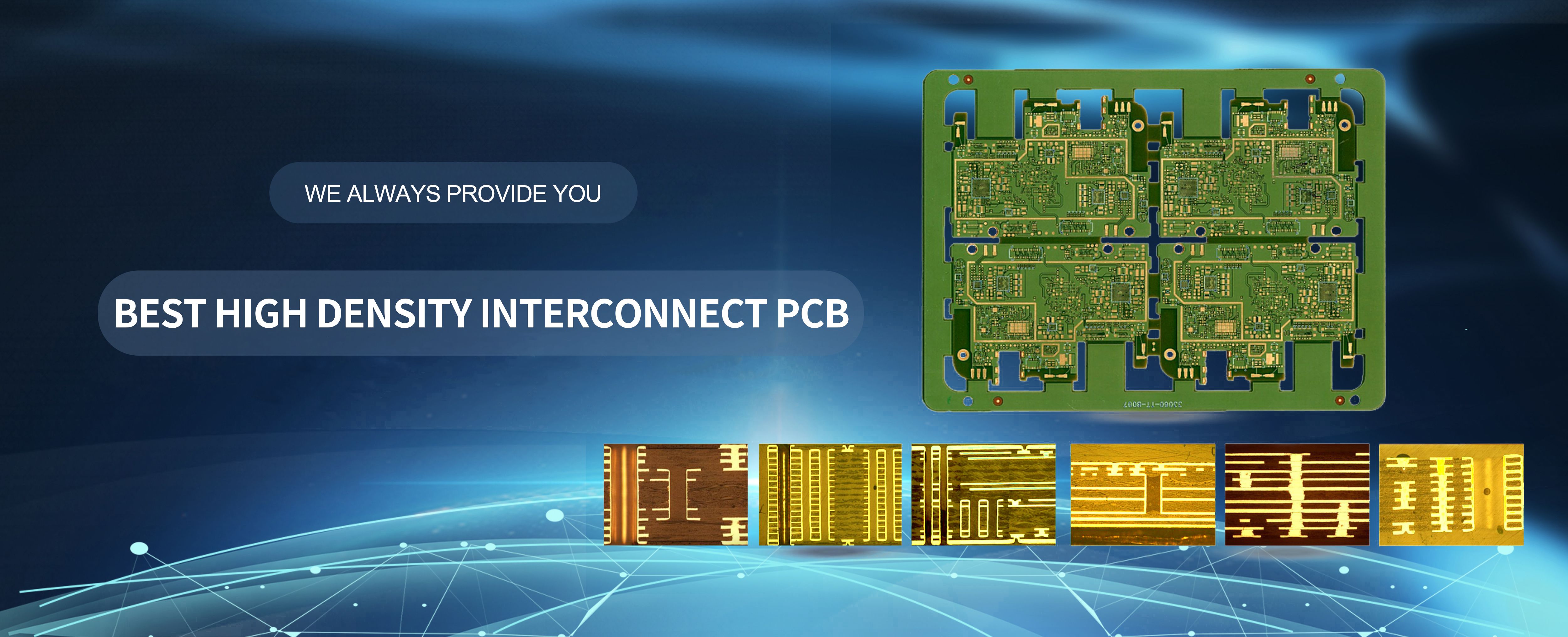
As PCBs continue to decrease in size and increase in complexity, your PCB fabricator has to keep up. As a designer, you certainly understand that old processes are revised and new ones are added, including those needed for High Density Interconnect (HDI). As your PCB fabricator, O-LeadingPCB is always working to stay ahead of the game!HDI is one of O-LeadingPCB’s specialties. HDI requires more than fine lines in the foil pattern; it also requires Sequential Build-Up(SBU), and laser-drilled Micro-Vias.
Sequential Build-Up
Multilayer
technology using SBU involves the addition of one layer of dielectric and foil
pattern at a time, allowing processing of HDI Micro-Vias before adding another
layer.
These layers are added to the substrate in pairs, one layer on each side of the
substrate, to balance the stresses to the substrate. For example, 1, 2, 3, etc.
layers on each side of the substrate (N), or 1+N+1, 2+N+2, 3+N+3, etc.
Laser-Drilled Micro-Vias
Laser-drilled Micro-Vias reduce the space required by through-the-board vias. They are smaller in diameter, and because of this, more space can be devoted to circuit traces.
A Micro-Via links only one layer of foil to the next; layers above and below them are available for foil lines, further increasing overall circuit density.
As each layer of SBU is added, a laser drills a hole from the outer layer of foil, through the dielectric that was just laid down, to the next inner layer of foil. This hole is then plated and filled. If there is an additional layer of SBU, the Micro-Via becomes buried.
Not all fabricators fill their Micro-Vias. O-leading fills the Micro-Vias with solid metal for stronger connections and to obtain better thermal management, increasing overall board reliability.
High density I/O components sometimes require Via-In-Pads (VIP) just to connect traces to all solder pads. When VIPs are used, filling the Micro-Via helps keep the pad smooth, allowing for a better reflow of solder.
Filling also allows the Micro-Vias to be stacked on top of each other to connect three or more layers of foil, further increasing density.
Contact O-Leading for more information about HDI technology at sales@o-leading.com

