


Capabilities: BGAs (Ball Grid Arrays):
BGAs, or Ball Grid Arrays, require special mounting practices. A BGA is a Surface Mounted Device (SMD) with a pattern, or array, of solder pads across its bottom side. Spheres of higher-temperature solder are attached to these pads, and take the place of ‘leads’ such as other types of components use to connect to the PCB. This ball configuration provides the flexibility that these components require during thermal cycling (hot/cold) without stressing the physical and electrical connections made by the balls between the component pads and the PCB land pattern.
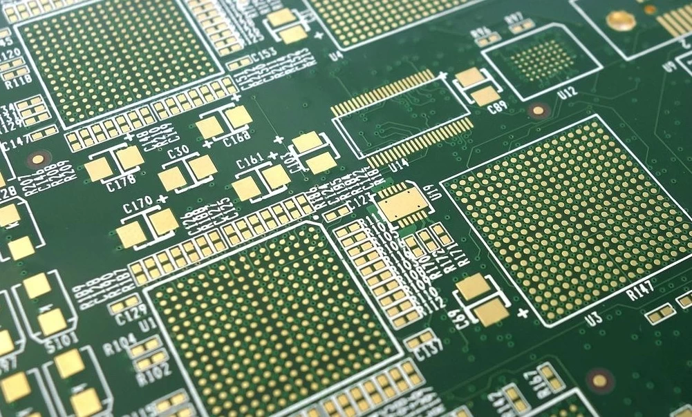
Attachment of the BGA to the PCB is made by stencil printing solder paste onto the PCB’s land pattern pads, then placing the BGA with its spheres attached onto the pattern, with the spheres contacting their corresponding pads and pressing into the solder paste. The BGA is then reflow soldered in a conveyorized oven. Since the solder paste alloy melts at a lower temperature than the BGA spheres, the paste melts and forms solder joints between the spheres and the PCB; the solder spheres are not allowed to melt.
The BGA provides a greater number of interconnections to the PCB than is available on a conventional quad-flat pack IC; this is the primary advantage of the BGA.
Assembly
The BGA provides a greater number of interconnections to the PCB than is available on a conventional quad-flat pack IC. It is precisely placed on the printed circuit board so the pads on the BGA match with the pads of the PCB.
The BGA and the PCB are then heated with just enough heat to reflow the solder, joining the BGA and the PCB together.
BGA Advantages
The BGA uses surface mount technology: it connects to top layer of the PCB only, allowing circuit traces to be routed underneath, and it provides for High Density Interconnections (HDI) with its efficient use of board space.
The leads, between the chip inside and the pads across the bottom of the chip, are shorter, allowing for greater speed with less inductance. Heat, too, is less of a problem because the BGA is soldered directly to the board, and the heat doesn’t have to go all the way to the edges of the IC, and down its leads, in order to be dissipated.
Among the uses for Ball Grid Arrays are audio, video, data storage and processing, communication equipment, medical equipment, radar/sonar, 3D graphics, and imaging.
Contact us at sales@o-leading.com for more information on Ball Grid Array technology.