
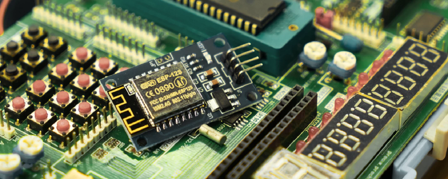


HDI PCB Manufacturing
With top advanced capabilities of competitive PCB market, we got high reputations of offering HDI PCB (printed circuit boards). HDI PCBs are the circuit boards with higher wire density than standard criterias. HDI PCBs appear thinner lines and spaces, smaller vias and higher connection pad density, which are commonly used for high spacing and precision required devices and system cards.
Our high HDI PCB boards have the technology-driving capabilities to bring applications in a large number of industries including but not limited to semiconductor test equipment, military weapons, medical, and aerospace.
Capabilities: HDI, High Density Interconnects
High-Density
Interconnects (HDI) are a fact of life in today’s miniaturized electronics
assemblies, such as smart devices and tablets.
HDI technology is incorporated
into the basic fabrication of the PCB itself and the connections to the
components.
The
HDI isn’t used just the connections between Printed
Circuit Boards (PCBs),
like the freeways connecting the cities; it’s in the
fabrication of the PCB
itself and the connections to the components, like the city streets and alleys
between the dwellings and apartment buildings.
Fine Pitch
Surface Mount Technology (SMT) with its fine pitch components requires the printed circuit board miniaturization characteristics and benefits of HDI:
• Tight
tolerances
• Densely spaced traces and pads
• Multiple layers on a single PCB
• Micro-vias to carry signals from one layer to another
HDI,
with its attendant reduction in size and weight, goes hand in hand with this
greater density of surface mount components. Of course,
the high count
connections for integrated circuits and components including BGAs and
flip chips simply adds to the need for HDI.
HDI Design Advantages
The
smaller size and weight of HDI circuitry means that the circuit boards fit into
smaller spaces and have less mass than conventional
printed circuit designs.
The smaller size and weight also contributes to less chance of damage from
mechanical shocks.
Considerations for HDI Assembly
Placement
of the components on the PCB requires more accuracy than conventional PCB
design due to the smaller, more
compact topography of the PCB.
BGAs and Flip Chips necessitate special soldering techniques and added steps in the assembly and rework (repair) process.
HDI at O-LEADING PCB
Our engineers will be pleased to assist you with the engineering and design of your HDI PCBs.
For more information, contact us at sales@o-leading.com.