


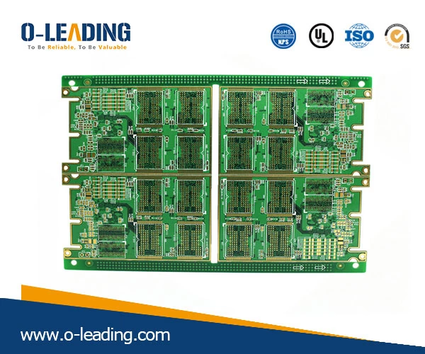
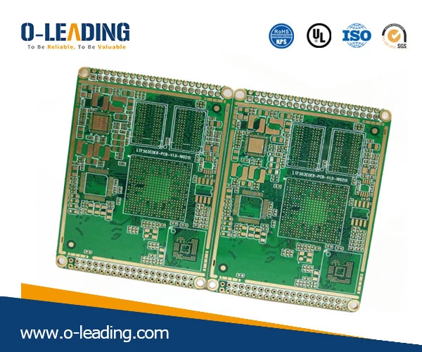
Some common problems in PCB design and cabling
o-leading.com
o-leading.com
2017-09-20 19:42:59
How to solve the contradiction between manual routing and automatic routing of high speed signals?
At present, most of the automatic cabling devices with strong cabling software have set constraints to control the winding mode and the number of vias. Each EDA company's winding engine capabilities and constraints setting projects sometimes differ greatly. For example, if there is enough hunting line control constraints (serpentine) winding, the ability to control the differential pair line spacing.
This can affect the way the wiring automatically comes in line with the designer's idea. In addition, manual adjustment of the ease of routing is also absolutely related to the ability of the winding engine. For example, the pushing capacity of the line, the ability to push through the hole, and even the pushing capacity of the wire to copper. So, it's a solution to choose a router that has a good ability to do the winding engine.
In the high-speed PCB design, the blank areas of the signal layer can be deposited with copper.
Most of the copper deposited in the blank area is grounded. Only when the copper is deposited near the high speed signal line, the distance between the deposited copper and the signal wire should be paid attention to, because the copper deposited will reduce the characteristic impedance of the wire. Also be careful not to affect the characteristic impedance of its layer, for example, in the structure of the dual strip line.
At present, most of the automatic cabling devices with strong cabling software have set constraints to control the winding mode and the number of vias. Each EDA company's winding engine capabilities and constraints setting projects sometimes differ greatly. For example, if there is enough hunting line control constraints (serpentine) winding, the ability to control the differential pair line spacing.
This can affect the way the wiring automatically comes in line with the designer's idea. In addition, manual adjustment of the ease of routing is also absolutely related to the ability of the winding engine. For example, the pushing capacity of the line, the ability to push through the hole, and even the pushing capacity of the wire to copper. So, it's a solution to choose a router that has a good ability to do the winding engine.
In the high-speed PCB design, the blank areas of the signal layer can be deposited with copper.
How should the copper layers in the multiple signal layers be allocated on the ground and the power supply?
Most of the copper deposited in the blank area is grounded. Only when the copper is deposited near the high speed signal line, the distance between the deposited copper and the signal wire should be paid attention to, because the copper deposited will reduce the characteristic impedance of the wire. Also be careful not to affect the characteristic impedance of its layer, for example, in the structure of the dual strip line.