


The difference between HDI board and ordinary PCB
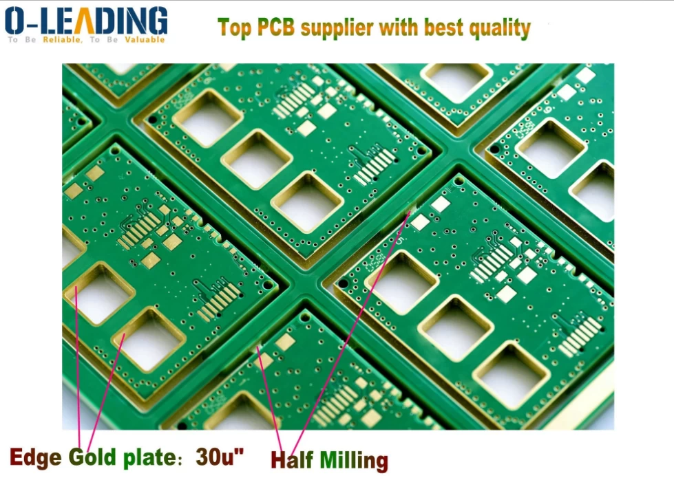
HDI board (High Density Interconnector), that is, high-density interconnector, is a circuit board with a relatively high line distribution density using micro-blind buried hole technology. The HDI board has inner layer circuit and outer layer circuit, and then uses drilling, metallization in the hole and other processes to realize the connection inside each layer of circuit.
HDI boards are generally manufactured using a lamination method. The more laminations, the higher the technical level of the board. Ordinary HDI boards are basically laminated one time. High-level HDI adopts the laminated technology of two or more times. At the same time, it adopts advanced PCB technologies such as stacked holes, electroplated hole filling, and laser direct drilling.
customization HDI PCB Printed Circuit Boards
When the density of the PCB increases more than eight layers, it will be manufactured with HDI, and its cost will be lower than that of the traditional complicated lamination process. HDI board is conducive to the use of advanced construction technology, its electrical performance and signal accuracy are higher than traditional PCB. In addition, HDI board has better improvement on radio frequency interference, electromagnetic wave interference, electrostatic discharge, heat conduction, etc.
Electronic products are constantly developing towards high density and high precision. The so-called "high" not only improves the performance of the machine, but also reduces the size of the machine. High-density integration (HDI) technology can make the design of end products more compact, while meeting higher standards of electronic performance and efficiency. At present, many popular electronic products, such as mobile phones, digital (camera) cameras, notebook computers, automotive electronics, etc., use HDI boards. With the replacement of electronic products and market demand, the development of HDI boards will be very rapid.
General PCB Introduction
PCB (Printed Circuit Board), the Chinese name is printed circuit board, also known as printed circuit board, is an important electronic component, a support for electronic components, and a carrier for the electrical connection of electronic components. Because it is made using electronic printing, it is called a "printed" circuit board.
Its main function is that after the electronic equipment adopts the printed board, due to the consistency of the same printed board, the error of manual wiring is avoided, and the automatic insertion or placement of electronic components, automatic soldering, and automatic detection can be realized to ensure Improve the quality of electronic equipment, improve labor productivity, reduce costs, and easy maintenance.
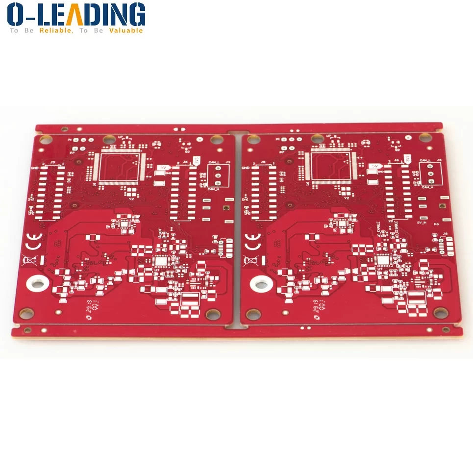
FR-4 UL approved led pcb board prototype fabrication
Are pcb boards with blind buried holes called hdi boards?
The HDI board is a high-density interconnection circuit board. The blind hole plating and the second lamination board are HDI boards, which are divided into first-order, second-order, third-order, fourth-order, and fifth-order HDI. For example, the iPhone 6 motherboard is fifth-order. HDI.
Simply buried holes are not necessarily HDI. How to distinguish HDI PCB first order and second order and third order
The first order is relatively simple, and the process and process are well controlled.
The second order started to be troublesome, one was the alignment problem, and the other was a hole punching and copper plating problem. There are many second-order designs:
One is the staggered position of each order. When the next-neighbor layer needs to be connected, it is connected to the middle layer through a wire, which is equivalent to two first-order HDI.
The second is that the two first-order holes overlap and the second-order is realized by superposition. The processing is similar to the two first-order, but there are many process points to be specially controlled, which are mentioned above.
The third method is to directly punch from the outer layer to the third layer (or N-2 layer). The process is different from the previous one, and the drilling is more difficult.
For the third order, the analogy is the second order.
The difference between HDI board and ordinary PCB
The common PCB board is mainly FR-4, which is made of epoxy resin and electronic grade glass cloth. Generally, the traditional HDI uses adhesive copper foil on the outermost layer. Because laser drilling can not penetrate the glass cloth, it is generally necessary to use glass fiber-free adhesive copper foil, but the current high-energy laser drilling machine can already penetrate 1180 glass cloth . This makes no difference from ordinary materials.