


How to consider safe spacing in PCB design?
There are many places in PCB design that need to consider the safety clearance. Here, it is temporarily classified into two categories: one is the electrical safety distance, and the other is the non-electricity safety distance.
Electrically relevant safety distance
1. Spacing between wires
As far as the processing capabilities of mainstream PCB manufacturers are concerned, the minimum distance between the wire and the wire should not be less than 4mil. The minimum line spacing is also the line-to-line and line-to-pad distance. From a production point of view, the bigger the better if possible, the more common is 10mil.
2. Pad aperture and pad width
As far as the processing capabilities of mainstream PCB manufacturers are concerned, if the pad aperture is mechanically drilled, the minimum should not be less than 0.2mm, if it is laser drilling, the minimum should not be less than 4mil. The aperture tolerance is slightly different according to the plate. It can generally be controlled within 0.05mm, and the minimum width of the pad should not be less than 0.2mm.
3. The distance between the pad and the pad
As far as the processing capabilities of mainstream PCB manufacturers are concerned, the distance between pads and pads should not be less than 0.2mm.
4. The distance between the copper skin and the edge of the board
The distance between the charged copper skin and the edge of the PCB board is preferably not less than 0.3mm. Set this spacing rule on the Design-Rules-Board outline page.
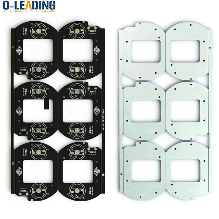
SMD LED Bulb PCB Circuit Board Module 12W
If copper is laid on a large area, there is usually a shrinkage distance from the edge of the board, which is generally set to 20mil. In the PCB design and manufacturing industries, under normal circumstances, due to mechanical considerations of the finished circuit board, or to avoid the possibility of curling or electrical short circuit caused by the exposed copper strip on the edge of the board, engineers often lay large areas of copper The block shrinks by 20 mils relative to the edge of the board, instead of laying the copper skin all the way to the edge of the board.
There are many ways to deal with this kind of copper shrinkage, such as drawing a keepout layer on the edge of the board, and then setting the distance between the copper and keepout. A simple method is introduced here, which is to set different safety distances for copper laying objects. For example, the safety distance of the whole board is set to 10mil, and the copper laying is set to 20mil, which can achieve the effect of shrinking the board edge by 20mil. The dead copper that may appear in the device is removed.
Non-electrical safety distance
1. Character width height and spacing
The text film can not be changed during processing, but the width of the character line with D-CODE less than 0.22mm (8.66mil) is bolded to 0.22mm, that is, the width of the character line L = 0.22mm (8.66mil).
The width W of the entire character is 1.0 mm, the height H of the entire character is 1.2 mm, and the spacing D between the characters is 0.2 mm. When the text is less than the above standard, the processing and printing will be blurred.
2. Distance from via to via
Via (VIA) to via spacing (hole edge to hole edge) is preferably greater than 8mil.
oem customized rohs pcb supplier
3. Distance from silk screen to pad
The silk screen is not allowed to cover the pad. If the silk screen is covered with pads, the tin will not be tinned when soldering, which will affect the placement of components. The general board factory requires a reservation of 8mil spacing as well. If the PCB area is really limited, the 4mil pitch is barely acceptable. If the silk screen accidentally covers the pad during design, the board manufacturer will automatically eliminate the silk screen portion left on the pad during manufacturing to ensure tin on the pad.
Of course, the specific circumstances of the specific analysis at the time of design. Sometimes the silk screen is deliberately close to the pad, because when the two pads are close to each other, the silk screen in the middle can effectively prevent the solder connection from shorting during soldering, which is another matter.
4. Mechanical 3D height and horizontal spacing
When mounting the components on the PCB, it is necessary to consider whether there will be conflicts with other mechanical structures in the horizontal direction and space height. Therefore, when designing, it is necessary to fully consider the adaptability between components, PCB products and product shells and the spatial structure, and reserve a safe distance for each target object to ensure that there is no conflict in space.