


The 8 classic problems of PCB (on)
Problem 1: PCB board short circuit
The biggest cause of PCB short circuit is the improper design of the solder pad. At this time, the round solder pad can be changed to an ellipse to increase the distance between points to prevent short circuit.
Inappropriate design of the direction of PCB parts will also cause the board to short circuit and fail to work. If the SOIC feet are parallel to the tin wave, it is easy to cause a short circuit accident. At this time, the direction of the part can be modified appropriately to make it perpendicular to the tin wave.
There is also a possibility that it will also cause short-circuit failure of the PCB, that is, the automatic plug bending foot. IPC stipulates that the length of the leg is less than 2mm and that the parts will fall off when the angle of the bent leg is too large, so it is easy to cause a short circuit, and the solder joint needs to be more than 2mm away from the line.
In addition to the three reasons mentioned above, there are some reasons that can also cause short circuit failures of the PCB board, such as too large substrate holes, too low temperature of the tin furnace, poor solderability of the board surface, solder mask failure, board Surface pollution, etc., are all common causes of failure. Engineers can compare and eliminate the above reasons and failure conditions one by one.
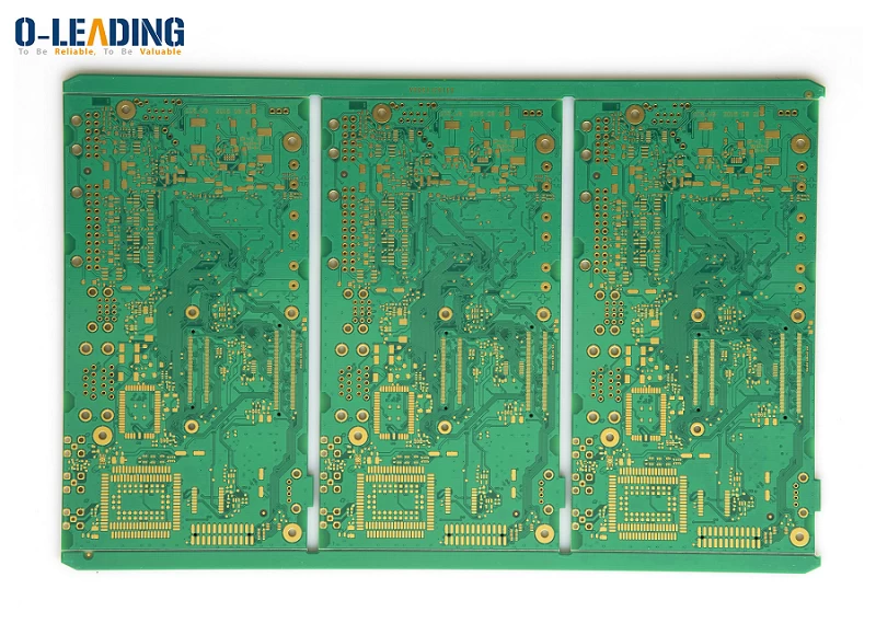
universal FR4 Multilayer PCB washing machine computer control board
Problem 2: dark and granular contacts appear on the PCB
The dark or small-grained contact problems on the PCB are mostly due to the contamination of the solder and the excessive amount of oxides mixed in the molten tin, resulting in a solder joint structure that is too brittle. Care must be taken not to be confused with the dark colors caused by the use of solder with low tin content.
Another reason for this problem is that the composition of the solder itself used in the manufacturing process has changed, the impurity content is too much, and it is necessary to add pure tin or replace the solder. The stained glass causes physical changes in the fiber buildup, such as separation between layers. But this situation is not a bad solder joint. The reason is that the substrate is heated too high, and it is necessary to reduce the preheating and soldering temperature or increase the speed of the substrate.
Question 3: PCB solder joints become golden yellow
Under normal circumstances, the solder of the PCB board is silver gray, but occasionally there are golden solder joints. The main reason for this problem is that the temperature is too high, at this time only need to lower the temperature of the tin furnace.
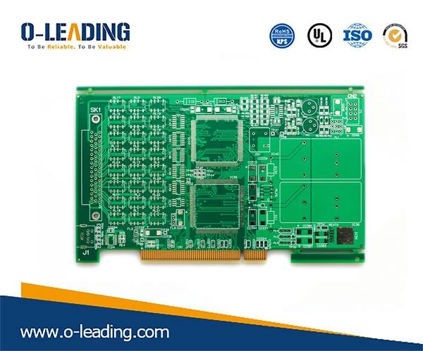
multilayer PCB manufacturer in china
Question 4: The badness of the board is also affected by the environment
Due to the structure of the PCB itself, when in an unfavorable environment, it is easy to cause damage to the PCB board. Extreme temperature or variable temperature, excessive humidity, high-intensity vibration and other conditions are all factors that cause the board performance to deteriorate or even be scrapped. For example, changes in ambient temperature can cause board deformation. This will destroy the solder joints, bend the shape of the board, or may cause the copper traces on the board to break.
On the other hand, moisture in the air can cause oxidation, corrosion, and rust on metal surfaces, such as exposed copper traces, solder joints, pads, and component leads. The accumulation of dirt, dust or debris on the surface of components and circuit boards will also reduce the air flow and cooling of the components, resulting in PCB overheating and performance degradation. Vibration, dropping, hitting or bending the PCB will deform it and cause the crack to appear, while high current or overvoltage will cause the PCB to break down or cause rapid aging of components and pathways.