


PCB stackup design
Before designing a multi-layer PCB circuit board, the designer needs to first determine the structure of the circuit board used according to the circuit size, circuit board size and electromagnetic compatibility (EMC) requirements, that is, decide whether to use 4, 6 or More layers of circuit board. After determining the number of layers, determine the placement of the internal electrical layers and how to distribute different signals on these layers. This is the choice of multilayer PCB stack structure. The stacked structure is an important factor that affects the EMC performance of the PCB board, and also an important means to suppress electromagnetic interference. This section will introduce the relevant content of the multilayer PCB laminate structure. After determining the number of power and ground layers and the number of signal layers, the relative arrangement between them is a topic that every PCB engineer cannot avoid;
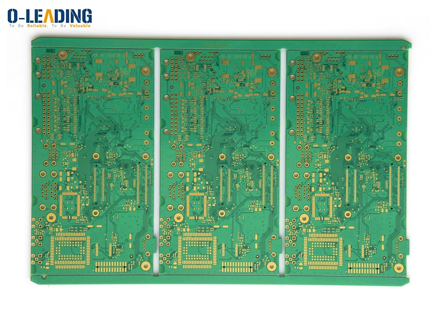
universal FR4 Multilayer PCB washing machine computer control board wholesale
General principles of layer arrangement:
1. Determining the stacking structure of multilayer PCBs requires more considerations. In terms of wiring, the more layers, the better the wiring, but the cost and difficulty of the board will also increase. For manufacturers, whether the stacked structure is symmetrical or not is the focus of attention in the manufacture of PCB boards, so the selection of the number of layers needs to consider the needs of various aspects to achieve the best balance. For experienced designers, after completing the pre-layout of components, they will focus on the PCB bottleneck. Combine with other EDA tools to analyze the wiring density of the circuit board; then combine the number and type of signal lines with special wiring requirements such as differential lines and sensitive signal lines to determine the number of signal layers; then according to the type of power supply, isolation and anti-interference Requirements to determine the number of inner electrical layers. In this way, the number of layers of the entire circuit board is basically determined.
2. Under the component surface (second layer) is the ground plane, providing the device shielding layer and providing the reference plane for the top layer wiring; the sensitive signal layer should be adjacent to an internal electrical layer (internal power supply/ground layer). Copper film to provide shielding for the signal layer. The high-speed signal transmission layer in the circuit should be the intermediate layer of the signal, and it is sandwiched between the two inner electrical layers. In this way, the copper films of the two inner electrical layers can provide electromagnetic shielding for high-speed signal transmission, and can also effectively limit the high-speed signal radiation between the two inner electrical layers without causing interference to the outside.
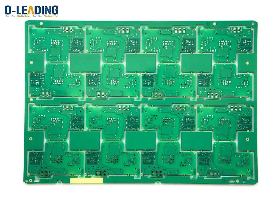
OEM manufacture Multilayer+PCB Board Printed Circuit Boards PCB fabrication
3. All signal layers should be as close as possible to the ground plane;
4. Try to avoid the two signal layers directly adjacent to each other; crosstalk is easily introduced between adjacent signal layers, resulting in circuit function failure. Adding a ground plane between the two signal layers can effectively avoid crosstalk. 5. The main power supply is as close as possible to its counterpart;
6. Consider the symmetry of the laminated structure.
7. For the layer arrangement of the mother board, it is difficult to control the parallel long-distance wiring of the existing mother board. For the board-level operating frequency above 50MHZ (for conditions below 50MHZ, please refer to the appropriate relaxation), the recommended layout principle:
*The component surface and welding surface are complete ground plane (shield);
*No adjacent parallel wiring layer;
*All signal layers are as close as possible to the ground plane;
*The key signal is adjacent to the stratum and does not cross the partition.
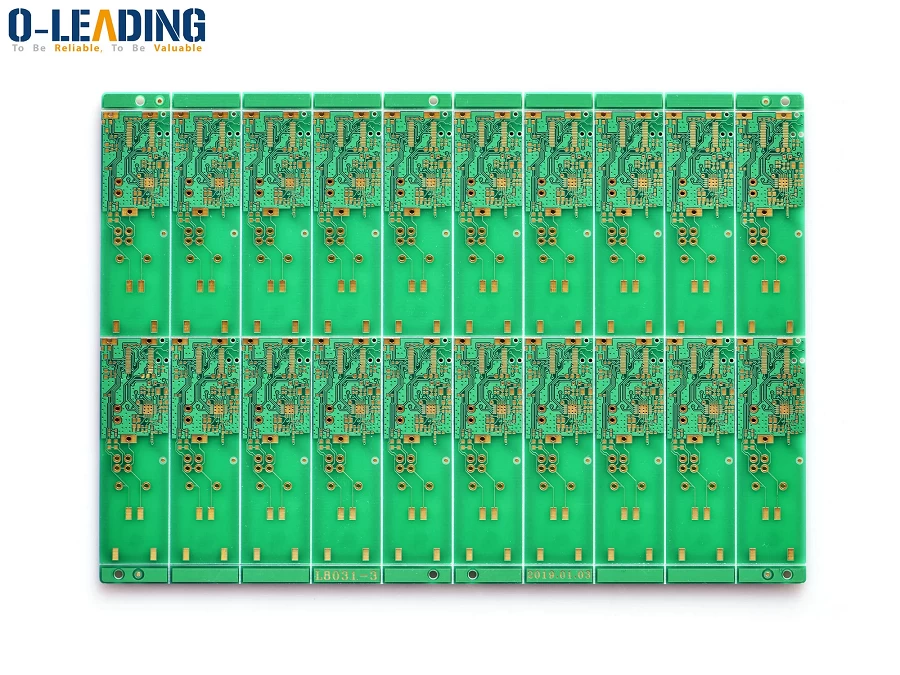
FR4 Rigid Double layer PCB manufacture China
Note: When setting the specific PCB layers, you must flexibly grasp the above principles. On the basis of understanding the above principles, according to the actual board requirements, such as: whether a critical wiring layer, power supply, and ground plane division are required To determine the arrangement of the layers, don't move them hard, or hold on.
8. Multiple grounded inner electrical layers can effectively reduce the grounding impedance. For example, the A signal layer and the B signal layer use separate ground planes, which can effectively reduce common mode interference.