


PCB impedance control
Different routing methods can be calculated to obtain the corresponding impedance values.
Microstrip line
• It consists of a strip conductor and a ground plane with a dielectric in between. If the dielectric constant of the dielectric, the width of the line, and its distance from the ground plane are controllable, its characteristic impedance is also controllable and its accuracy will be within ±5%.
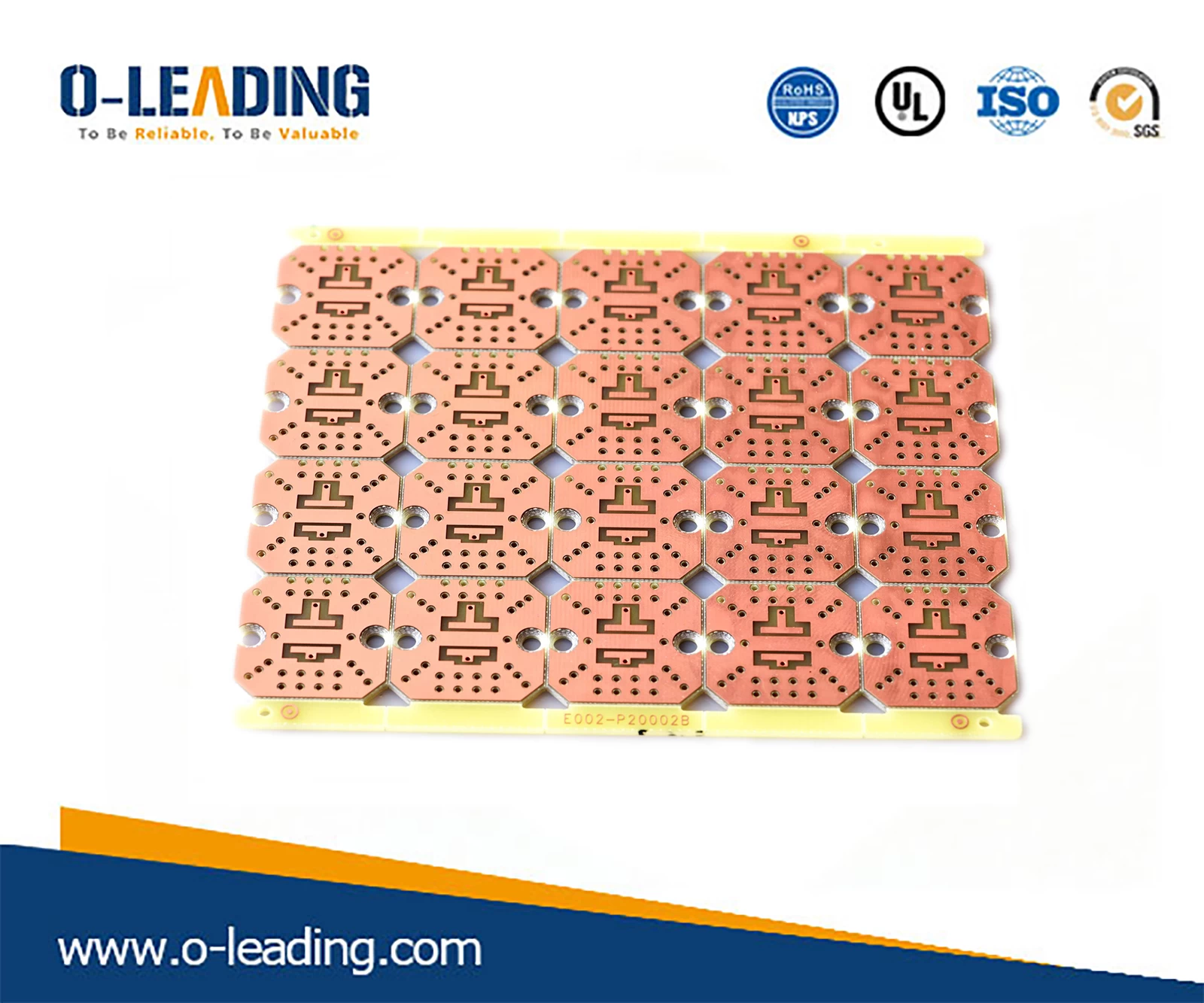
Copper Based PCB manufacturer china.
Stripline
A stripline is a strip of copper placed between the dielectric layers between two layers of conductive planes. If the thickness and width of the line, the dielectric constant of the dielectric, and the distance between the two ground planes are all controllable, the characteristic impedance of the line is also controllable with an accuracy of 10%.
The structure of the multi-layer board:
In order to control the impedance of the PCB well, we must first understand the structure of the PCB:
Generally speaking, the multi-layer board is made by laminating and laminating the core board and the prepreg. The core board is a hard, specific thickness, two-bread copper sheet, which is the basic material constituting the printed board. . The prepreg constitutes a so-called wetting layer which acts to bond the core sheet, although it also has a certain initial thickness, but its thickness will change somewhat during the pressing process.
Power supply module manufacturer china.
Usually, the outermost two dielectric layers of the multilayer board are both wetting layers, and a separate copper foil layer is used as the outer copper foil on the outside of the two layers. The original thickness specifications of the outer copper foil and the inner copper foil are generally 0.5OZ, 1OZ, 2OZ (1OZ is about 35um or 1.4mil), but after a series of surface treatments, the final thickness of the outer copper foil is generally Will increase by nearly 1OZ. The inner copper foil is the copper on both sides of the core plate, and the final thickness is very small from the original thickness, but due to etching, it is generally reduced by several um.
The outermost layer of the multilayer board is a solder mask, which is what we often call "green oil". Of course, it can also be yellow or other colors. The thickness of the solder mask is generally not easy to determine accurately. The area without copper foil on the surface is slightly thicker than the area with copper foil. However, because of the lack of thickness of the copper foil, the copper foil still appears more prominent when we use It can be felt when the finger touches the surface of the printed board.