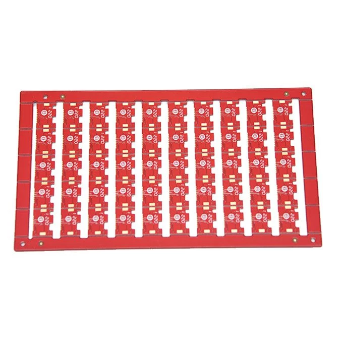
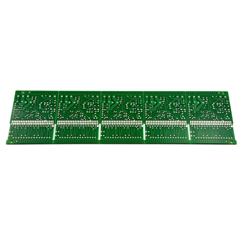
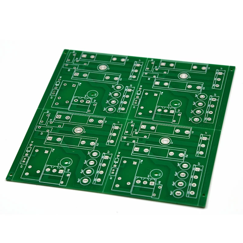
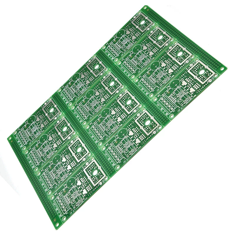
Main principles of wiring in PCB design
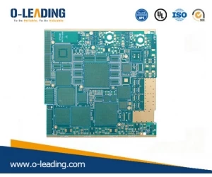
China Mobile phone pcb board manufacturer
Wiring is the most important process in the overall PCB design. This will directly affect the performance of the PCB. In the PCB design process, the wiring generally has three levels of division: the first is the cloth, which is the most basic requirement for PCB design. If the line is not laid, and the line is flying, it will be an unqualified board. Second is the satisfaction of electrical performance. This is a measure of the eligibility of a printed circuit board. This is after the connection, carefully adjust the wiring to achieve the best electrical performance. Then it is beautiful. If your wiring is connected, there is no place that affects the performance of the electrical appliances, but at a glance, in the past, with a lot of colorful, colorful, then how good your electrical performance is, in the eyes of others is still a piece of garbage. This brings great inconvenience to testing and maintenance. The wiring should be neat and uniform, and there should be no rules. These must be achieved while ensuring the electrical performance and meeting other individual requirements, otherwise it will be the end.
1. Main principles when wiring
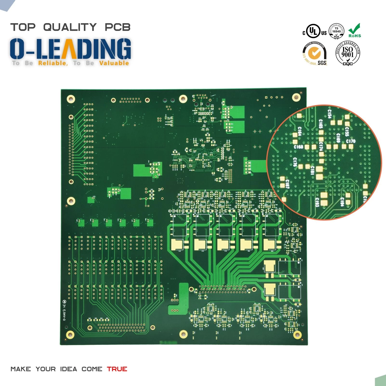
1 In general, the power and ground wires should be routed first to ensure the electrical performance of the board. Within the scope of the conditions, try to widen the power supply and ground line width. It is better to ground the ground line than the power line. Their relationship is: ground line > power line > signal line. Usually the signal line width is 0.2~0.3mm. The finest width can reach 0.05~0.07mm, and the power cord is generally 1.2~2.5mm. For the PCB of the digital circuit, a wide ground wire can be used to form a loop, that is, a ground net is used.
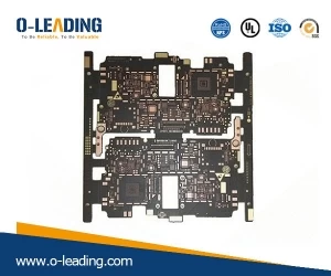
2 Pre-wire the more demanding lines, and the edges of the input and output should avoid adjacent parallel to avoid reflection interference. If necessary, ground wire should be isolated. The wiring of two adjacent layers should be perpendicular to each other, and parasitic coupling is easy to occur in parallel.
3 The oscillator case is grounded, the clock line should be as short as possible, and it should not be anywhere. Below the clock oscillating circuit, the special high-speed logic circuit part should increase the area of the ground, and should not take other signal lines, so that the surrounding electric field approaches zero;
4 Use 45o polyline wiring as much as possible, and do not use 90o polyline to reduce the radiation of high frequency signals;(Key board PCB supplier china)
5 Do not form a loop on any signal line. If it is unavoidable, the loop should be as small as possible; the signal line should have as few vias as possible;
6 The critical lines are as short and thick as possible, with protective ground on both sides.
7 When transmitting sensitive signals and noise field signals through a flat cable, use “ground-signal-ground” to extract.
8 Key signals should be reserved for test points to facilitate production and maintenance testing.


