


Electrical rules to be noted throughout the PCB design
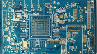
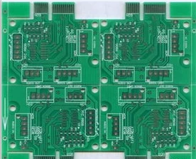
china Mobile phone pcb manufacturer
1, power, ground processing
Even if the wiring in the entire PCB board is completed well, the interference caused by the inconsistency of the power supply and the ground line may degrade the performance of the product, and sometimes even affect the success rate of the product. Therefore, the wiring of electricity and ground wire should be taken seriously, and the noise interference generated by electricity and ground wire should be minimized to ensure the quality of the product.
For every engineering engineer engaged in the design of electronic products, the reason for the noise between the ground and the power line is known. Now, only the reduced noise suppression is expressed: it is known to add between the power supply and the ground. Coupling capacitor. Try to widen the power supply and ground line width. It is better to ground the ground line than the power line. Their relationship is: ground line > power line > signal line. Usually the signal line width is 0.2~0.3mm, and the finest width is up to 0.05~0.07mm, the power cable is 1.2~2.5mm. For the PCB of the digital circuit, a wide ground wire can be used to form a loop, that is, a ground net is used to use (the ground of the analog circuit cannot be used in this way). For the wire, the place that is not used on the printed board is connected to the ground as the ground wire. Or make a multi-layer board, power supply, ground line each occupy a layer.
2. Co-processing of digital circuits and analog circuits
Many PCBs are no longer single-function circuits, but a mixture of digital and analog circuits. Therefore, it is necessary to consider the mutual interference between them when wiring, especially the noise interference on the ground.
The frequency of the digital circuit is high, and the sensitivity of the analog circuit is strong. For the signal line, the high-frequency signal line is as far as possible away from the sensitive analog circuit device. For the ground line, the whole human PCB has only one node to the outside, so The problem of processing numbers and common ground must be performed inside the PCB, and the digital ground and the analog ground inside the board are actually separated from each other, but only at the interface where the PCB is connected to the outside world. The digital ground is slightly shorted to the analog ground. Please note that there is only one connection point. There is also no common ground on the PCB, which is determined by the system design.
3. The signal line is laid on the electrical layer.
In the wiring of multi-layer printed boards, since there are not many lines left in the signal line layer, the addition of layers will cause waste and increase the workload for production, and the cost will increase accordingly. To resolve this contradiction, consider wiring on the electrical layer. The power layer should be considered first, followed by the ground layer. Because it is best to preserve the integrity of the formation.
4. Treatment of connecting legs in large-area conductors
In a large area of grounding (electricity), the legs of common components are connected to them, and the treatment of the connecting legs needs to be comprehensively considered. In terms of electrical performance, the pads of the component legs are perfectly connected with the copper surface, but There are some hidden dangers in the soldering assembly of the components. For example, 1 welding requires a high-power heater. 2 is easy to cause a virtual solder joint. Therefore, taking into account the electrical performance and process needs, the crucible pad is called the thermal isolation commonly known as the thermal pad, so that the possibility of creating a solder joint due to the excessive heat of the cross section during soldering is greatly reduced. The treatment of the electrical layer legs of the multilayer board is the same.(oem pcb board manufacturer china)
5, the role of the network system in the wiring
In many CAD systems, cabling is determined by the network system. The mesh is too dense, although the path is increased, but the stepping is too small, the data volume of the field is too large, which inevitably has higher requirements on the storage space of the device, and the computing speed of the object computer electronic product is also Great impact. Some of the paths are invalid, such as occupied by the pads of the component legs or occupied by the mounting holes and the holes. The grid is too sparse, and too few paths have a great impact on the routing rate. Therefore, there must be a sparse and reasonable grid system to support the wiring.