


Layout requirements for special devices in PCB design
PCB device layout is not a freewheeling thing, it has certain rules that everyone needs to follow. In addition to general requirements, some special devices also have different layout requirements.
Layout Requirements for Crimp Devices
1) There should be no higher than 3mm components around 3mm of the crimp / male and bend / female crimping device surfaces, and there should be no soldering devices around 1.5mm; the reverse side of the crimping device is 2.5 away from the center of the pinhole of the crimping device There must be no components within the range of mm.
2) Straight / male and straight / female crimping devices must not have any components around 1mm; when a sheath is required on the back of straight / male and straight / female crimping devices, no element shall be arranged within 1mm from the edge of the sheath. For components, no components shall be arranged within 2.5mm from the crimping hole when the sheath is not installed.
3) The live plug connector of the grounding connector used with European-style connectors. The front end of the long pin is 6.5mm and the short pin is 2.0mm.
4) The long pin of the single PIN pin of 2mmFB power supply corresponds to the 8mm forbidden cloth at the front end of the board socket.
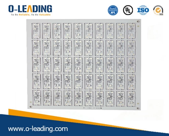
Single Side Aluminum Base Board
Layout requirements for thermal devices
1) In the layout of the device, the thermal sensitive devices (such as electrolytic capacitors, crystal oscillators, etc.) should be kept as far away as possible from the high thermal devices.
2) The thermal sensor should be close to the tested component and away from the high temperature area, so as not to be affected by other heating work equivalent components and cause malfunction.
3) Place the heat-generating and heat-resistant device near the air outlet or on the top, but if it cannot withstand high temperature, also place it near the air inlet, and try to rise with other heat-generating and thermal-sensitive devices in the air as much as possible Staggered in direction.
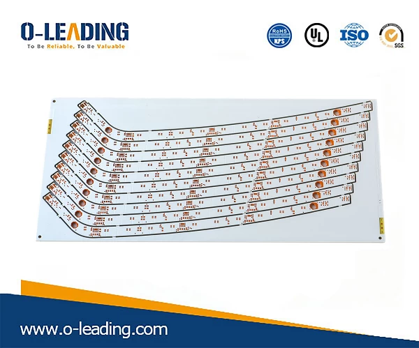
Single Side Aluminum Base Board
Layout requirements with polar devices
1) THD devices with polarity or directionality are aligned in the same direction and arranged neatly.
2) The orientation of polar SMC is as consistent as possible on the board; the devices of the same type are arranged neatly and beautifully.
(Polar devices include: electrolytic capacitors, tantalum capacitors, diodes, etc.)
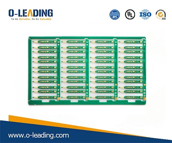
LED Lighting manufacturer china
Layout requirements for through-hole reflow devices
1) For PCBs with a non-transmitting edge size greater than 300mm, heavier devices should not be placed in the middle of the PCB to reduce the impact of the weight of the inserted device on the PCB deformation during the soldering process, and the board's Impact of placed devices.
2) To facilitate insertion, the device is recommended to be placed near the operation side of the insertion.
3) It is recommended that the length of the longer device (such as a memory socket) be consistent with the transmission direction.
4) The distance between the edge of the through hole reflow soldering device and the QFP, SOP, connector and all BGAs with pitch ≤ 0.65mm is greater than 20mm. The distance to other SMT devices is> 2mm.
5) The distance between the body of the through-hole reflow soldering device is> 10mm.
6) The distance between the edge of the pad of the through-hole reflow soldering device and the transmission side is ≥10mm; the distance from the non-transmission side is ≥5mm.