


In PCB design, you need to understand these common mistakes.
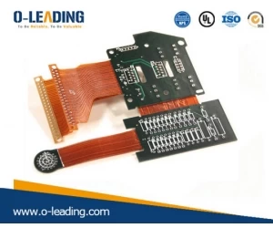
LED strip pcb Pcb manufacturer
When you use Licence EDA to complete PCB layout and check that the network and DRC have not reported an error, is a PCB completed? The answer is of course no. Many beginners also include experienced engineers who have neglected post-examination due to tight time or impatience or overconfidence. There are some very basic bugs in the results. Here are some of the most basic and most error-prone elements to post-check.
1, component packaging
(1) Pad pitch. If it is a new device, you must draw the component package yourself to ensure proper spacing, and the pad pitch directly affects the soldering of the component.
(2) Via size (if any). For plug-in devices, the via size should be reserved with sufficient margin.
(3) Contour silk screen. The outline screen of the device is preferably larger than the actual size to ensure that the device can be installed smoothly.
2, layout
(1) The IC should not be near the edge of the board.
(2) Devices of the same module circuit should be placed close to each other. For example, the decoupling capacitor should be close to the power supply pin of the IC. The devices that make up the same functional circuit are placed in an area with a clear hierarchy to ensure the realization of the function.
(3) Arrange the position of the socket according to the actual installation. The sockets are all lead wires to other modules. According to the actual structure, in order to facilitate the installation, the proximity principle is generally adopted, and the position of the socket is arranged, and generally close to the edge of the board.(china Mobile phone pcb board manufacturer)
(4) Pay attention to the direction of the socket. The sockets are all oriented, the direction is reversed, and the wires are re-customized. For flat-plug sockets, the socket orientation should be towards the outside of the board.
(5) The source of interference should be kept away from sensitive circuits. High-speed signals, high-speed clocks, or high-current switching signals are all sources of interference and should be kept away from sensitive circuits such as reset circuits and analog circuits.
OEM Pcb prototype manufacturer china
3, wiring
(1) Line width size. The line width should be selected in combination with the process and current carrying capacity. The minimum line width cannot be less than the minimum line width of the PCB manufacturer. At the same time ensure the ability to carry current.
(2) Differential signal line. For differential lines such as USB and Ethernet, note that the traces should be of equal length, parallel, and plane, and the spacing is determined by the impedance.
(3) Pay attention to the return path of the high-speed line. High-speed lines are prone to electromagnetic radiation. If the path between the trace path and the return path is too large, a single-turn coil will form a radiated electromagnetic interference. Therefore, when routing, pay attention to the return path next to it. The power board and ground plane of the multi-layer board can effectively solve this problem.
(4) Pay attention to the analog signal line. The analog signal line should be separated from the digital signal. The trace should be avoided as far as possible from the source of interference, and the shorter the trace, the better.