Impedance matching method in PCB design
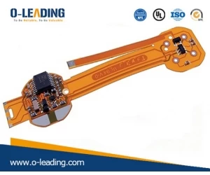
china Mobile phone pcb board manufacturer
1, tandem terminal matching
Under the condition that the signal source impedance is lower than the characteristic impedance of the transmission line, a resistor R is connected in series between the source end of the signal and the transmission line, so that the output impedance of the source end matches the characteristic impedance of the transmission line, and the signal reflected from the load end is suppressed. Re-reflection occurred.
Matching resistor selection principle: The sum of the matching resistor value and the output impedance of the driver is equal to the characteristic impedance of the transmission line. Common CMOS and TTL drivers, whose output impedance varies with the level of the signal. Therefore, for TTL or CMOS circuits, it is impossible to have a very correct matching resistor, which can only be considered. The signal network of the chain topology is not suitable for series termination matching, and all loads must be connected to the end of the transmission line.
Series matching is the most common method of terminal matching. It has the advantage of low power consumption, no additional DC load on the driver, no additional impedance between the signal and ground, and only one resistor component.
Common applications: impedance matching of general CMOS and TTL circuits. The USB signal is also sampled by this method for impedance matching.
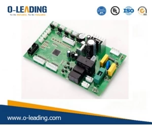
LED strip pcb Pcb manufacturer
2, parallel terminal matching
In the case where the impedance of the signal source is small, the input impedance of the load end is matched with the characteristic impedance of the transmission line by increasing the parallel resistance, so as to eliminate the reflection at the load end. The implementation form is divided into two forms: single resistance and double resistance.
Matching resistance selection principle: In the case of a high input impedance of the chip, for a single resistance form, the parallel resistance value of the load terminal must be close to or equal to the characteristic impedance of the transmission line; for the dual resistance form, each parallel resistance value It is twice the characteristic impedance of the transmission line.(led pcb board supplier china)
The advantage of parallel termination matching is simple and easy. The obvious disadvantage is that it will bring DC power consumption: the DC power consumption of the single resistance mode is closely related to the duty cycle of the signal; the dual resistance mode is whether the signal is high or low. There is DC power consumption, but the current is less than half of the single resistor.
Common applications: more applications with high-speed signals.


