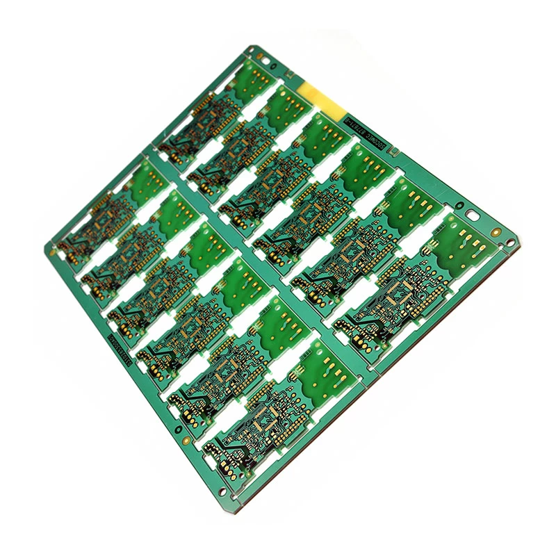
Tips for PCB design

multilayer manufacturer in China
1. What is the relationship between the line width and the size of the via on the PCB and the current flowing through it?
A typical PCB has a copper foil thickness of 1 ounce, and a line width of approximately 1 mm allows a maximum current of 1 A. The via hole is more complicated, in addition to the size of the via pad, and also related to the thickness of the copper wall after plating.
2. How to improve the routing rate?
To complete the design of a printed board diagram, it is generally necessary to pass the schematic input - network table generation - define the process of Keepout Layer - network table (component) loading - component layout (manual) wiring.(oem pcb board Printed company)
3. If there are only four DDRmemory stickers on the motherboard, the clock can be up to 150MHz. What are the specific requirements for wiring?
150MHz clock routing, it is required to minimize the length of the transmission line and reduce the impact of the transmission line on the signal. If you still can't meet the requirements, simulate it and see if the matching, topology, impedance control and other strategies are effective.
4. After the automatic floating copper, the floating copper will fill the blank according to the position of the device on the board and the layout of the trace?(HDI PCB manufacturer china)
However, this will form a lot of sharp angles and burrs less than or equal to 90 degrees. It will discharge during the high voltage test and cannot pass the high voltage test. I don't know that except for the automatic floating copper, the sharp corners and burrs are removed by manual correction. There is no other good way.
The problem of sharp copper floating in automatic floating copper is indeed a very troublesome problem. In addition to the discharge problem you mentioned, it will also cause processing problems due to acid droplet accumulation during processing.


