


How to make your PCB layout fast and look high
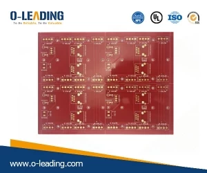
washing machine pcb board Printed circuit board
PCB layout is very important in the overall PCB design, how to make fast and efficient wiring, and make your PCB layout look tall, it is worth studying and studying. This article has compiled several aspects that need to be paid attention to in PCB layout. Come and check out the missing ones!
Co-processing of digital circuits and analog circuits
Many PCBs are no longer single-function circuits, but a mixture of digital and analog circuits. Therefore, it is necessary to consider the mutual interference between them when wiring, especially the noise interference on the ground.
The frequency of the digital circuit is high, and the sensitivity of the analog circuit is strong. For the signal line, the high-frequency signal line is as far as possible away from the sensitive analog circuit device. For the ground line, the whole human PCB has only one node to the outside, so The number of processing and the common ground must be handled inside the PCB, and the digital ground and the analog ground inside the board are actually separated from each other, but only at the interface where the PCB is connected to the outside (such as a plug).
The digital ground is slightly shorted to the analog ground. Please note that there is only one connection point. There is also no common ground on the PCB, which is determined by the system design.
Signal wires are laid on the power or ground plane
In the wiring of multi-layer printed boards, since there are not many lines left in the signal line layer, the addition of layers will cause waste and increase the workload for production, and the cost will increase accordingly. To resolve this contradiction, consider wiring on the power plane or ground plane.(High quality pcb wholesales)
Treatment of connecting legs in large-area conductors
In a large area of grounding or power supply, the legs of common components are connected to them. The handling of the connecting legs needs to be considered comprehensively. In terms of electrical performance, the pads of the component legs are perfectly connected with the copper surface, but the components are There are some hidden dangers in the welding assembly. For example, welding requires a high-power heater; it is easy to cause a virtual solder joint.
Therefore, taking into account the electrical performance and process needs, the crucible pad is called the thermal isolation commonly known as the thermal pad, so that the possibility of creating a solder joint due to the excessive heat of the cross section during soldering is greatly reduced. The electrical connection of the multilayer board or the treatment of the formation legs is the same.