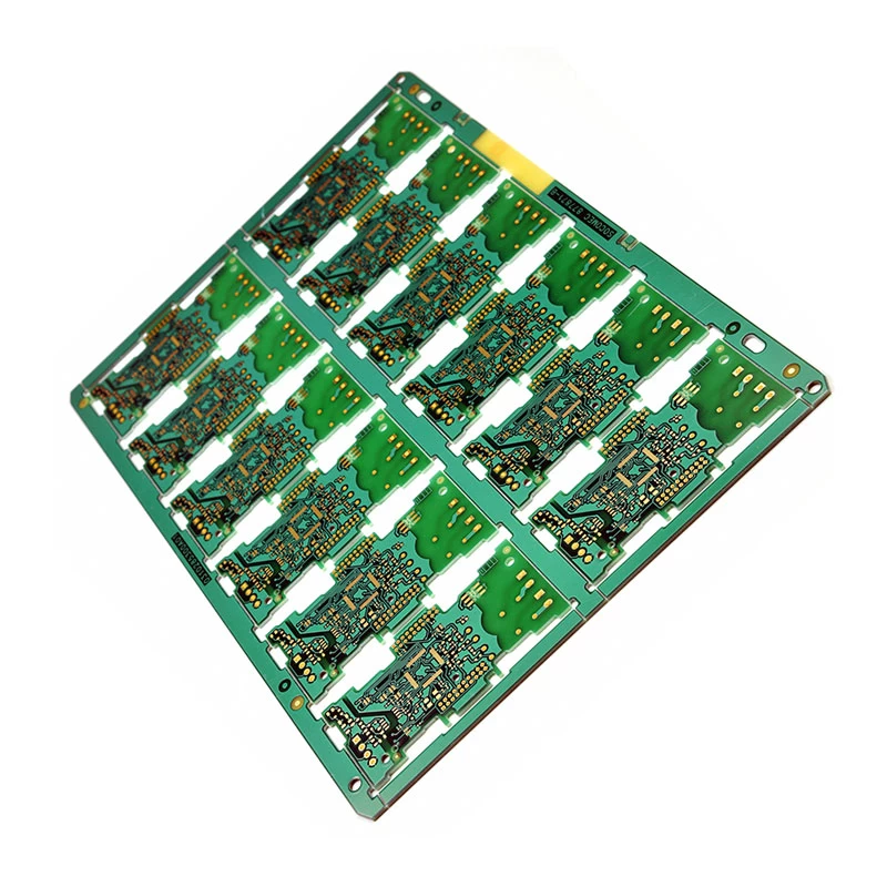
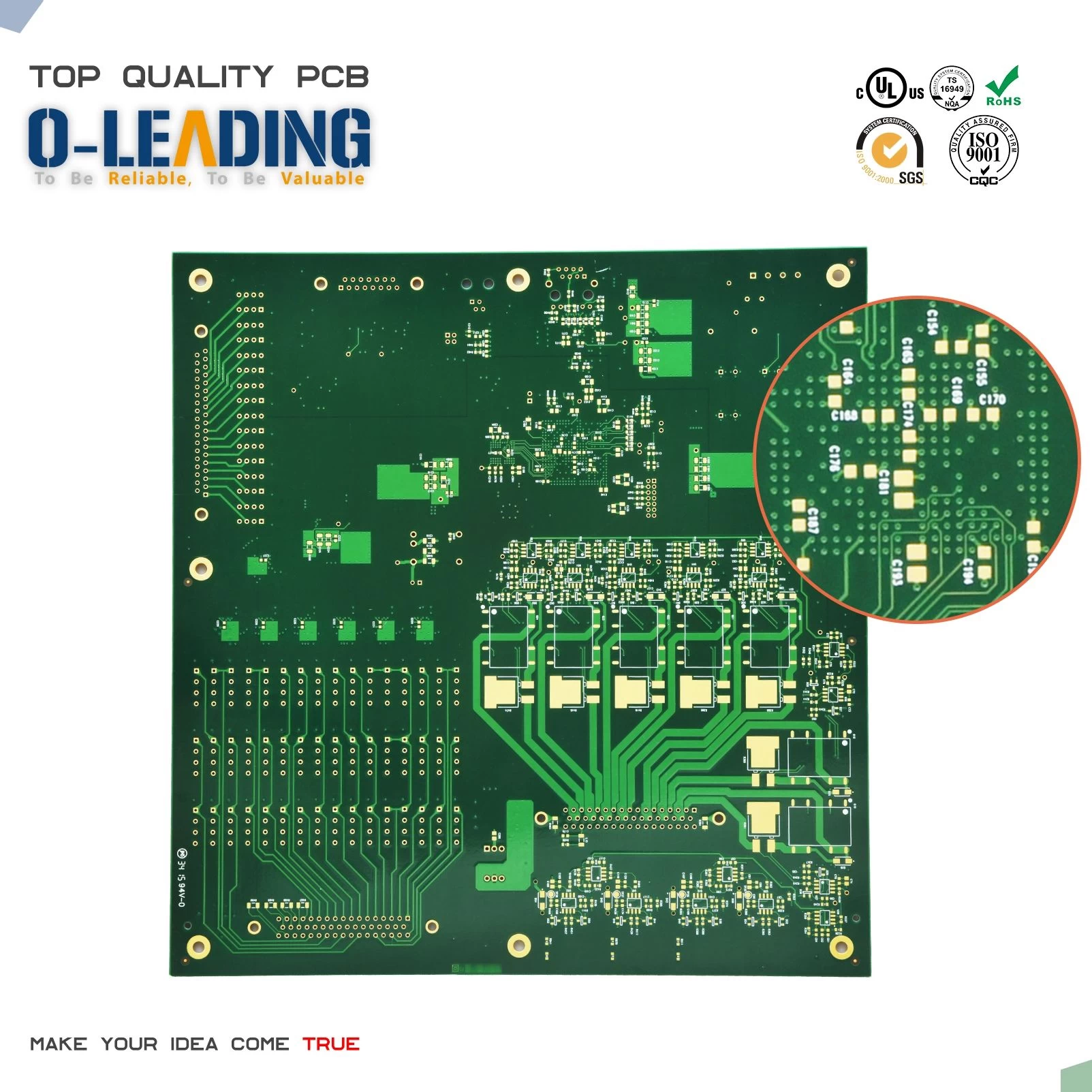
How should special components be laid out in a pcb design?
Printed circuit board manufacturer
China Mobile phone pcb board manufacturer
1 Try to reduce the wiring between high-frequency components as much as possible, and try to reduce their distribution parameters and mutual electromagnetic interference. Components that are susceptible to interference cannot be placed too close together, and input and output components should be kept as far away as possible.
2 Some components or wires may have a high potential difference, and the distance between them should be increased to avoid accidental short circuit caused by discharge. Components with high voltage should be placed as far as possible in the hands of the hand when debugging.
3 components weighing more than 15g should be fixed with brackets and then soldered. Those components that are large, heavy, and have a lot of heat should not be mounted on the printed board, but should be installed on the chassis of the whole machine, and heat dissipation should be considered. The thermal element should be kept away from the heating element.
4 For the layout of adjustable components such as potentiometer, adjustable inductor, variable capacitor, micro switch, etc., the structural requirements of the whole machine should be considered. If it is adjusted inside the machine, it should be placed on the printing plate for easy adjustment; if it is adjusted outside the machine, its position should be adapted to the position of the adjustment knob on the chassis panel.
5 Leave the position occupied by the positioning holes of the printing plate and the fixing bracket.

