How to better ensure signal integrity during PCB design
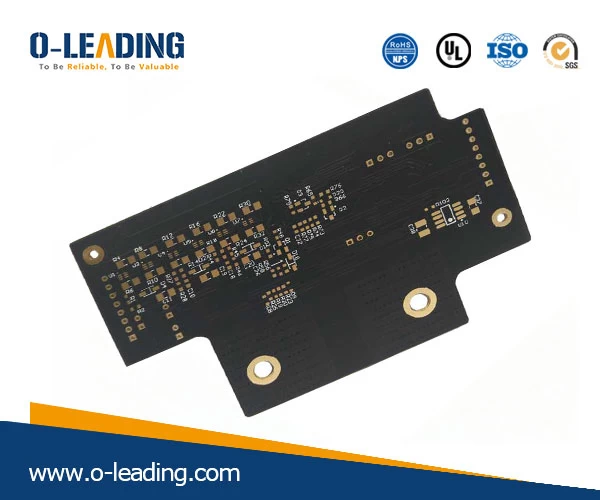
Printed circuit board manufacturer
In order to better ensure signal integrity in the PCB design process, you must consider the following aspects:
(1) Circuit design considerations. Including controlling the number of synchronous switching outputs, controlling the maximum edge rate of each unit to obtain the lowest and acceptable edge rate; selecting differential signals for high output function blocks; terminating passive components on the transmission line to achieve impedance between transmission lines and loads match.
(2) Minimize the trace length of the parallel wiring.
(3) The components should be placed away from the I/O interconnection interface and other areas susceptible to interference and coupling, and the spacing between components should be minimized.
(4) Shorten the distance between the signal traces to the reference plane.
(5) Reduce the trace impedance and signal drive level.
(6) Terminal matching. Terminal matching circuits or matching components can be added.
(7) Avoid parallel wiring of the traces, provide sufficient trace spacing between traces, and reduce inductive coupling.


