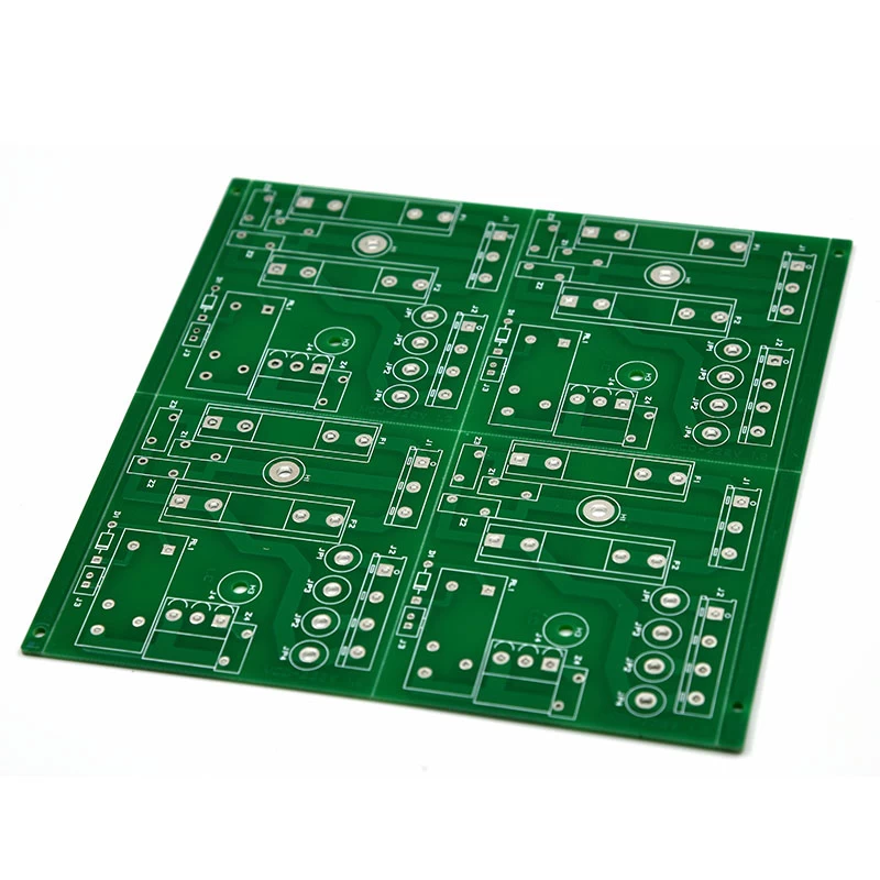
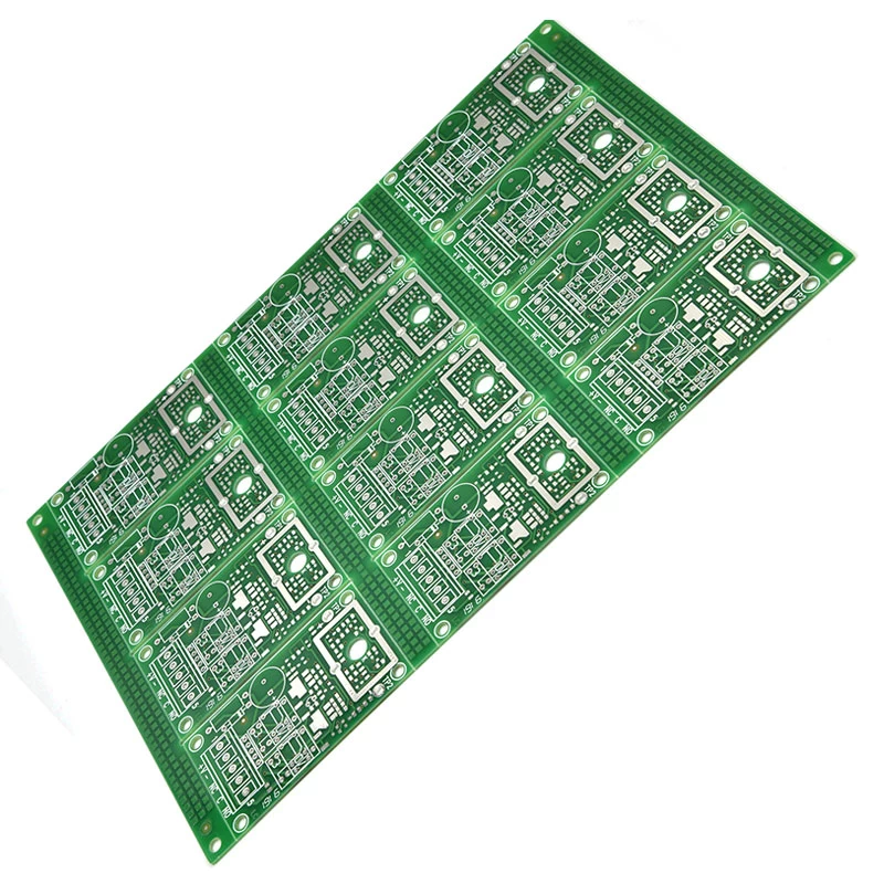
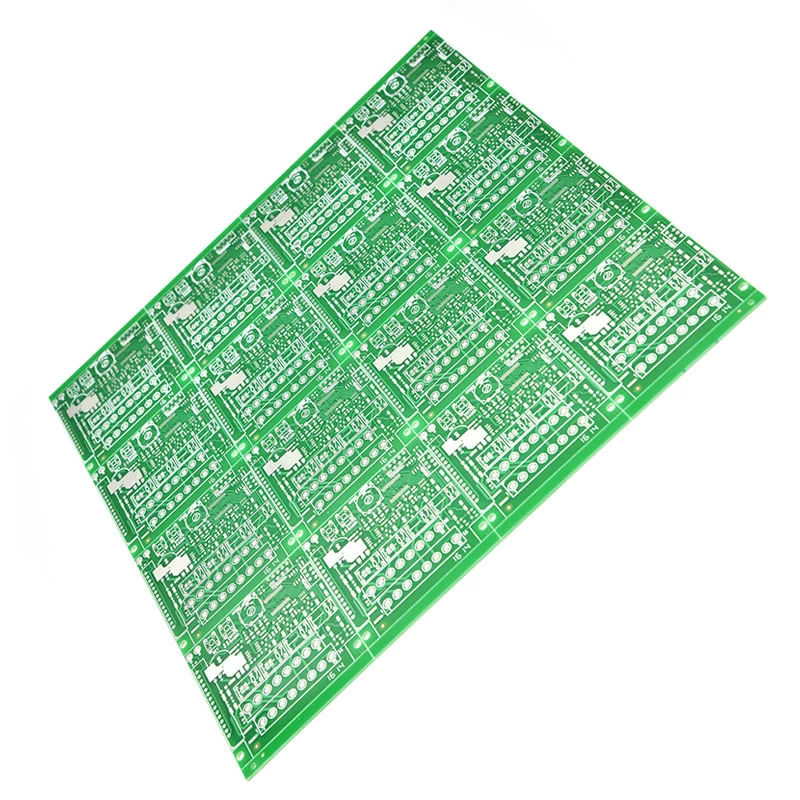
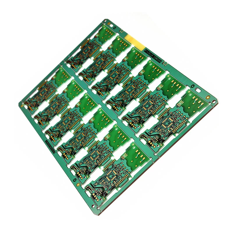
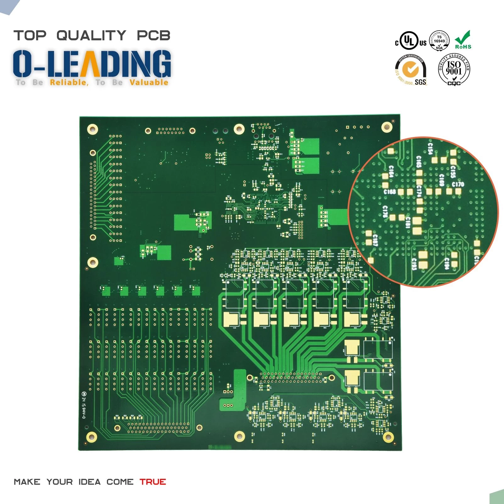
How to properly set the wire width in PCB design?

Multilayer pcb printed company
The width of the printed conductor in the PCB design should follow the following rules:
1, the wire width should be able to meet the electrical performance requirements and easy to produce, its minimum value depends on the current, but the minimum should not be less than 0.2mm, in the high-density, high-precision printed circuit, the wire The width and spacing are generally 0.3 mm.
2. The width of the wire should be considered in the case of high current. The single-panel experiment shows that when the copper foil thickness is 50μm, the wire width is 1-1.5mm, and the current is 2A, the temperature rise is very small. Therefore, generally use 1 A -1.5mm wide wire may meet PCB design requirements without causing temperature rise.
3. The common ground wire of the printed conductor should be as thick as possible. If possible, use a line larger than 2-3mm. This is especially important in circuits with microprocessors because the local line is too thin due to the flow of The change in current, the change in ground potential, and the unstable timing of the microprocessor timing signal can degrade the noise margin. (pcb board Printed company china)


