Factors affecting the effect of document maps in PCB copy boards
First, software technology
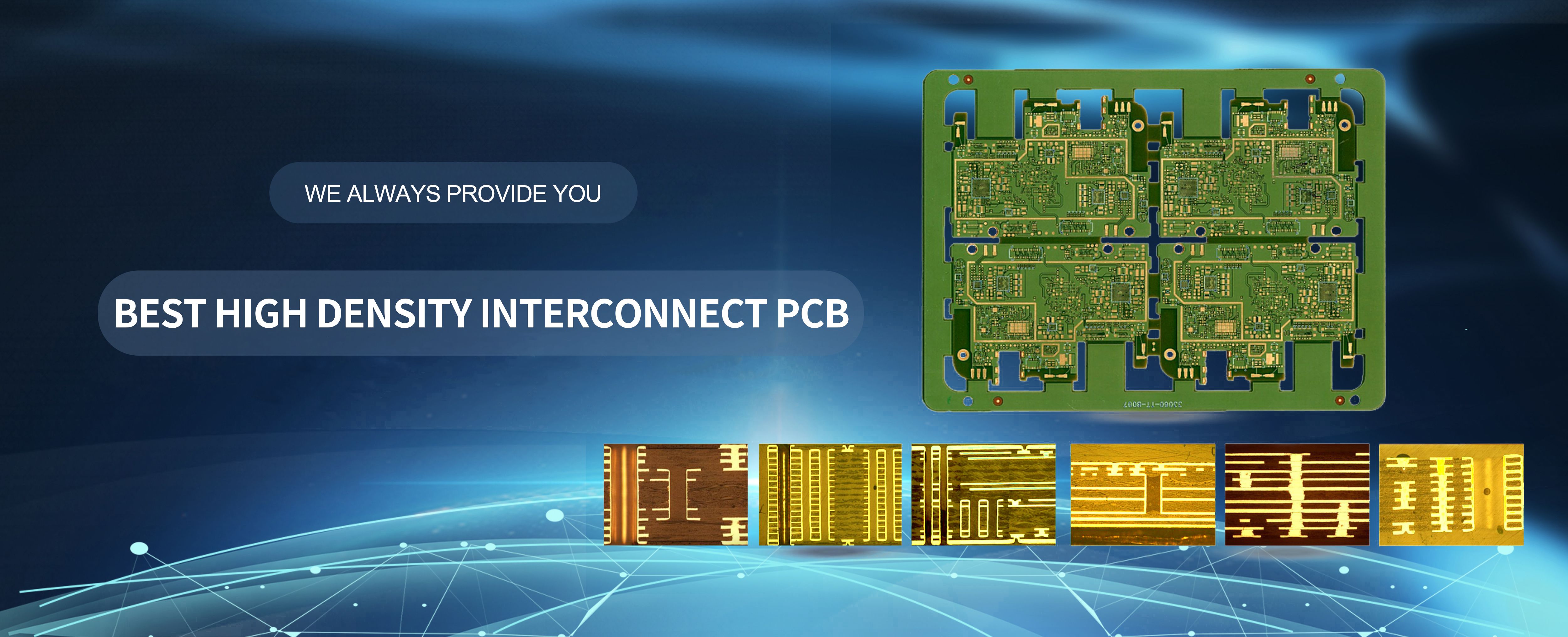
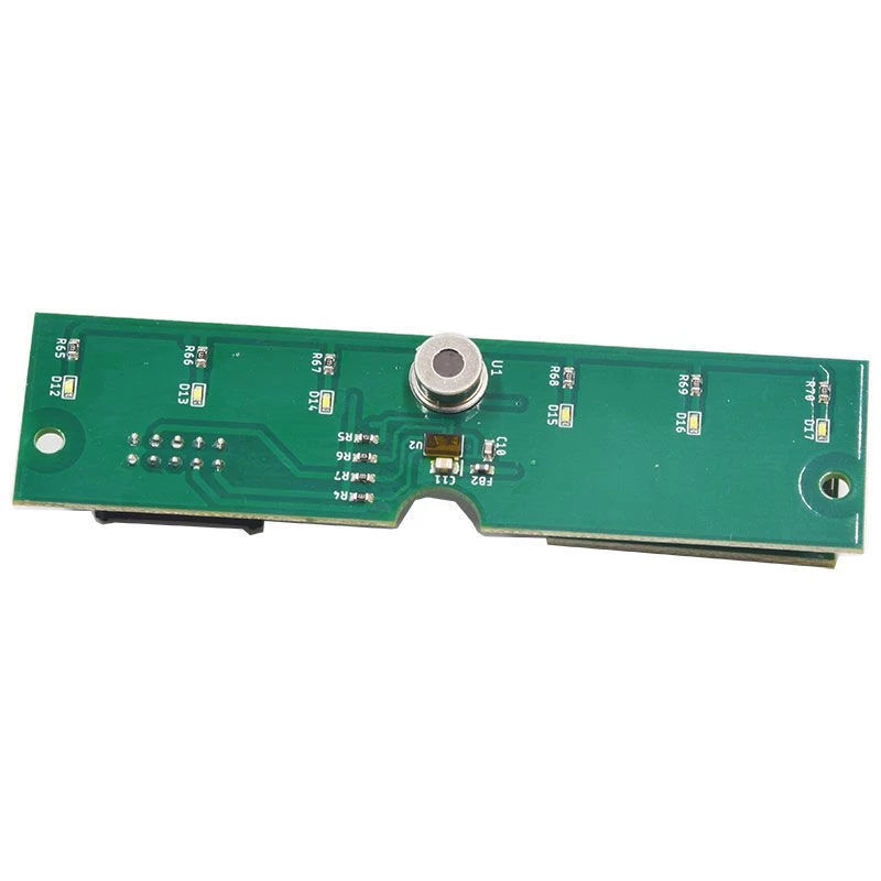
After the original PCB is scanned, according to the original image, the document drawing is required by means of the PCB copying software.
In terms of software type, we have a fully functional copy board software, which is important because the choice of software can be reflected in the final exported PCB layout and the resulting schematic.
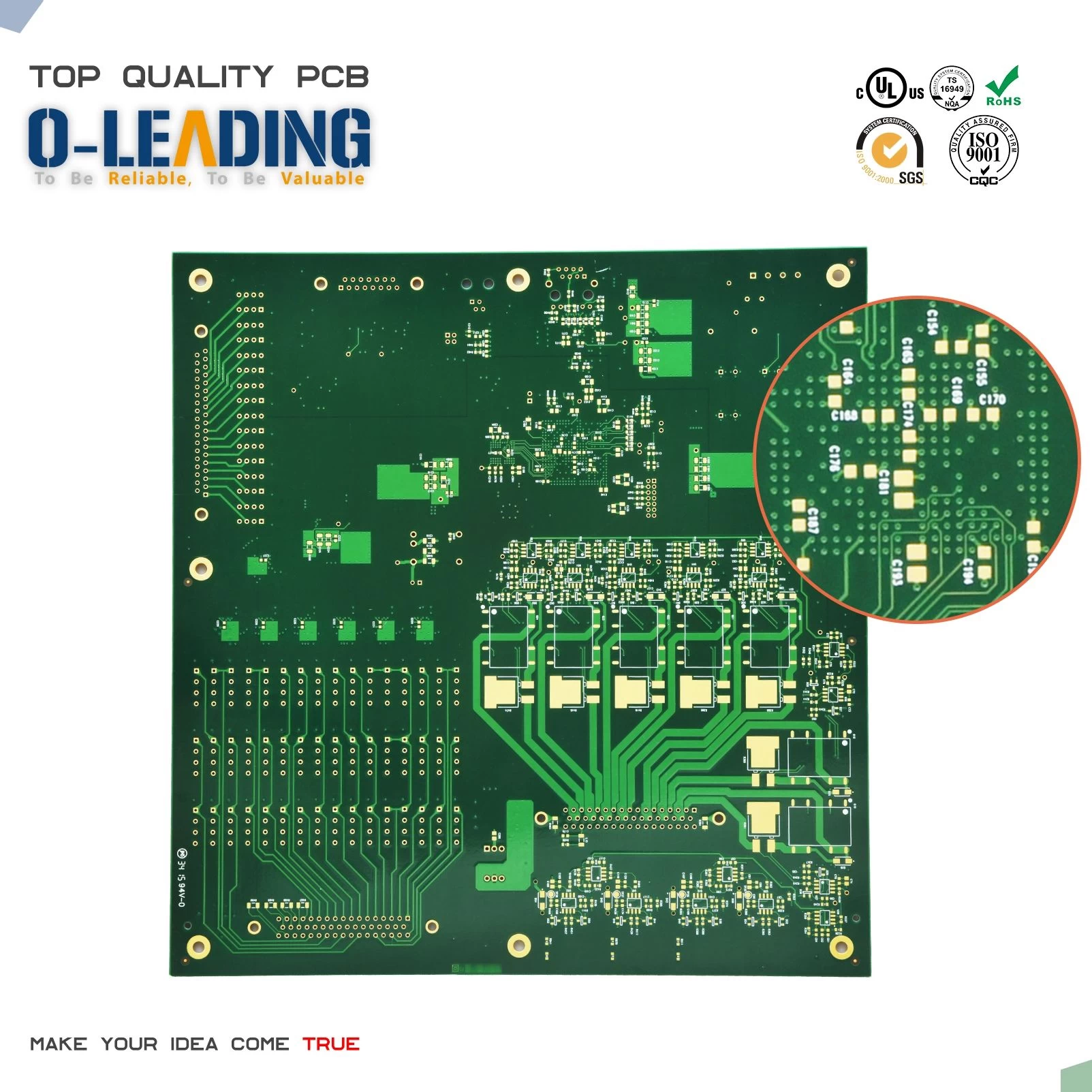
After selecting the well-functioning software, in order to ensure the perfect effect, the double-layer board and the multi-layer board copy board should also have rich experience and skill in technology. Because the same double-layer or multi-layer PCB board, the holes are in the same position, but the line connection is different, then when the original board wiring rules are drawn in the copy board software, the top-level PCB files that have been copied out of the double-layer board are stacked on the PCB board. On the scanned image of the other layer, the vias of the two overlap, and then the top line and the silk screen are not displayed, and another layer of the line is drawn according to the position of the via, so that the exported PCB file contains two sides of the double panel. data.
The same applies to the multi-layer board, except that the surface layer is sanded after the surface PCB file is drawn, so that the inner layer routing rules are exposed, and then copied by the same technique using the copy board software.
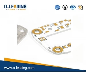
Aluminum Printed Circuit Boards in China
Advanced scanning technology, combined with mature software operation skills, strictly in accordance with the process of copying the board, you will find that the exported PCB file map or PCB electronic layout, in the routing rules, via location, line orientation and other parameters Will be consistent with the original PCB. On the contrary, any error in the middle of the link, whether it is the accuracy setting of the scanning process, or the decision and depiction of the routing rules and function modules by the copy board software, will affect the effect of the final PCB file map.
Second, the scanning process
Since the PCB copy board involves a problem of the accuracy of the copy board, for the circuit board with high precision requirements such as the mobile phone board, it is necessary to copy the high-precision PCB layout. In the scanning process, it is necessary to accurately select and design the scanner. First, first ensure the accuracy of the original scanned image. It can be said that the accuracy of the copy board mainly depends on the original scanning accuracy.
In the PCB copying process, PCB scanning is undoubtedly the first step in all processes. To get a good PCB, you must first scan the computer and back up the relevant parameters and the original PCB layout.
After the board is removed, the split PCB board is officially entered into the board copy stage. The first thing to do is to scan to store and record the PCB image. One thing to mention here is that in order to ensure that the relevant parameters on the PCB after scanning are clearly visible, the stains and residual tin on the surface of the PCB should be removed before scanning.
One thing to note is that the higher the accuracy of the scanned image, the larger the image, and the higher the hardware requirements. Therefore, in the DPI setting, it needs to be set according to the specific conditions of the original board to ensure the next steps of the copying process. Play the best results.
Third, the test file map
The test should also include testing the electronic technical performance of the PCB to ensure that it is functionally consistent with the original board. For the completed document map, in order to ensure the specification, the final step should also be tested. A method for detecting a double-panel file map is to print a two-layer document image on a transparent film with a laser printer, and then compare the film with the original plate to check whether they are consistent.

