


4 design techniques to reduce PCB electromagnetic interference
Therefore, electromagnetic interference (EMI) is a threat to the safety, reliability and stability of electronic equipment. When designing electronic products, the design of the PCB is critical to solving EMI problems.
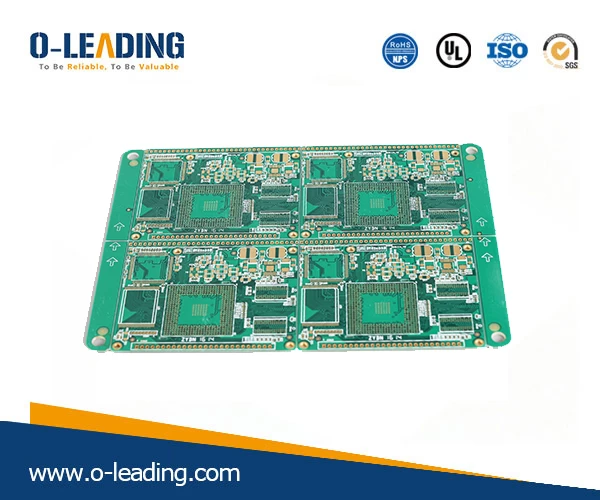
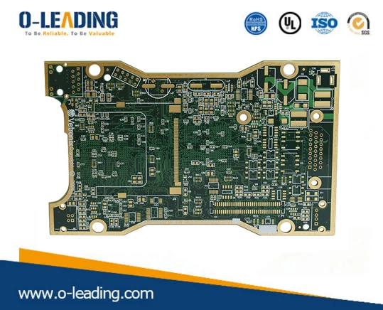
This article mainly explains the places to pay attention to when designing PCBs, thus reducing the electromagnetic interference problem in PCB boards. Multilayer PCB manufacturer in china.
Definition of electromagnetic interference (EMI)
Electromagnetic interference (EMI, Electro Magne TIc Interference) can be divided into radiation and conducted interference. Radiated interference is the interference source that uses space as a medium to interfere its signal with another electrical network. Conducted interference is the use of a conductive medium as a medium to interfere with signals on one electrical network to another. In high-speed system design, integrated circuit pins, high-frequency signal lines and various types of plugs are common sources of radiated interference in PCB design. The electromagnetic waves they emit are electromagnetic interference (EMI), which affects itself and other systems. normal work. 3D printer PCB supplier.
PCB board design techniques for electromagnetic interference (EMI)
There are many solutions to the EMI problem in today's PCB board design techniques, such as EMI suppression coatings, suitable EMI suppression parts, and EMI simulation designs. Now briefly explain these tips.
1. Common mode EMI interference source (such as the voltage drop formed by the transient voltage formed in the power busbar across the inductor of the decoupling path)
With low-value inductors in the power plane, the transients synthesized by the inductors are reduced and common-mode EMI is reduced.
Reduce the length of the power layer to IC power pin connections.
Use 3-6 mil PCB layer spacing and FR4 dielectric material.
China pcb manufacturers.
2, electromagnetic shielding
Try to place the signal traces on the same PCB layer and close to the power or ground plane.
The power plane should be as close as possible to the ground plane
3, the layout of the parts (different layouts will affect the circuit's interference and anti-interference ability)
Block processing according to different functions in the circuit (such as demodulation circuit, high-frequency amplifier circuit and mixing circuit, etc.), in which the strong and weak electrical signals are separated, and the digital and analog signal circuits are separated.
The filter network of each part of the circuit must be connected nearby, which not only reduces the radiation, but also improves the anti-interference ability of the circuit and reduces the chance of interference.
Components that are susceptible to interference should avoid interference sources such as CPU interference on the data processing board during layout.
4, wiring considerations (unreasonable wiring will cause cross interference between signal lines)
Do not have the traces close to the border of the PCB board to avoid disconnection during production.
The power line is wider and the loop resistance is reduced.
The signal lines are as short as possible and the number of vias is reduced.
The corner wiring should not be at right angles, and should be at 135° angle.
The digital circuit and the analog circuit should be isolated by ground, the digital ground and the analog ground should be separated, and finally connected to the power ground.
Reducing electromagnetic interference is an important part of PCB board design. As long as you go to this side of the design, you will naturally be more qualified in product tests such as EMC testing.