


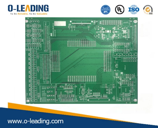
Etching process and process control of PCB
o-leading.com
o-leading.com
2017-08-14 13:39:09
The process of printed circuit boards from a light plate to a line pattern is a complex process of physical and chemical reactions. At present, the typical process of printed circuit board (power bank pcb board Printed) processing adopts graphical electroplating". In the first part of the board to keep the outer copper foil, which is part of the graphics circuit on pre plating a layer of tin resist layer, and then the rest of the copper foil etched by chemical etching method, called.
It should be noted that the board had two layers of copper on it. In the outer etching process, only one layer of copper must be etched off, and the rest will form the final circuit. This type of pattern is characterized by plating, copper plating layer only exists in the resist layer below tin.
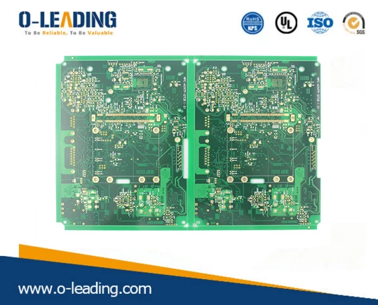
At present, tin or tin is the most commonly used anti corrosion layer, used in the etching process of ammonia etching agent. Ammonia etching agent is a chemical liquid medicine in common use, and tin or tin no chemical reaction. Ammonia etchant mainly refers to ammonia water / ammonia chloride etching solution.
It should be noted that the board had two layers of copper on it. In the outer etching process, only one layer of copper must be etched off, and the rest will form the final circuit. This type of pattern is characterized by plating, copper plating layer only exists in the resist layer below tin.
At present, tin or tin is the most commonly used anti corrosion layer, used in the etching process of ammonia etching agent. Ammonia etching agent is a chemical liquid medicine in common use, and tin or tin no chemical reaction. Ammonia etchant mainly refers to ammonia water / ammonia chloride etching solution.