


What are the causes of plate bending and plate warping during the PCB manufacturing process?
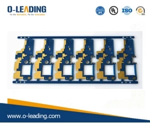
Double sided pcb manufacturer china
The reason why each plate bend and the plate warp may be different may be different, but it should be blamed that the stress applied to the board is greater than the stress that the board material can withstand, when the stress on the board is uneven or When the ability to resist stress is uneven in each place on the board, the result of plate bending and plate warping will occur. The following are the four major reasons for the plate bending and plate bending.
1. The area of the copper surface on the circuit board is not uniform, which will deteriorate the plate bending and the plate bending.
Generally, a large area of copper foil is designed for grounding. Sometimes the Vcc layer is also designed with a large area of copper foil. When these large areas of copper foil are not evenly distributed on the same circuit board. When it occurs, it will cause the problem of uneven heat absorption and heat dissipation. The circuit board will of course also expand and contract. If the expansion and contraction cannot cause different stresses and deformation at the same time, the temperature of the board has reached Tg. At the upper end of the value, the board will begin to soften, causing permanent deformation. (china High TG PCB supplier)
2. The weight of the circuit board itself will cause the board to be deformed
In general, the reflow oven uses a chain to drive the board forward in the reflow oven, that is, the two sides of the board are used as fulcrums to support the entire board. If the board has heavy parts or the size of the board is too large, It will show the phenomenon of the middle depression due to its own quantity, causing the plate to bend.
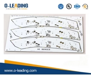
LED strip pcb Pcb manufacturer
3. The depth of the V-Cut and the connecting strip will affect the deformation of the panel.
Basically, V-Cut is the culprit in destroying the structure of the board. Because V-Cut cuts out V-shaped grooves on a large sheet of material, the V-Cut is prone to deformation.
4. The vias of the layers on the board will limit the board's expansion and contraction.
Most of today's circuit boards are multi-layer boards, and there are joints between the layers and the rivets. The connection points are divided into through holes, blind holes and buried holes. Where there are joints, the board is limited. The effect of rising and contracting will indirectly cause the plate to bend and the plate to be warped.