


Three major factors causing welding defects in PCB circuit board factory
PCB board welding technology In recent years, the development process of the electronics industry process, it can be noted that a very obvious trend is reflow soldering technology. The quality of PCB board soldering is also a concern of major electronics manufacturers. Let's take a look at the three major factors that cause PCB board soldering defects!
1. The solderability of PCB board holes affects the quality of soldering
The solderability of the PCB board hole is not good, and the solder joint defect will be generated, which will affect the parameters of the components in the circuit, resulting in unstable conduction of the multilayer board component and the inner layer line, causing the entire circuit function to fail. The so-called solderability is the property of the metal surface being wetted by the molten solder, that is, the metal surface of the solder forms a relatively uniform continuous smooth attached film.
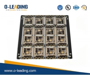
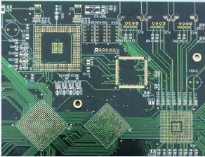
Printed Circuit Board PCB Manufacturing Company
2. Welding defects caused by warpage of PCB board
PCB boards and components are warped during soldering, and defects such as solder joints and short circuits are caused by stress deformation. Warpage is often caused by temperature imbalance between the upper and lower parts of the PCB. For large-sized PCB boards, warpage can occur due to their own weight drop. Ordinary PBGA devices are about 0.5mm away from the PCB. If the device on the PCB is large, the PCB will return to its normal shape after cooling down. The solder joint will be under stress for a long time. If the device is raised by 0.1mm, it will be enough to cause virtual Open the road.(PCB factory who export the goods to Europe)
3. PCB board design affects welding quality
In the layout, when the PCB size is too large, although the welding is easier to control, the printed lines are long, the impedance is increased, the noise resistance is reduced, and the cost is increased; when the temperature is too small, the heat dissipation is lowered, the welding is difficult to control, and adjacent lines are prone to occur. Mutual interference, such as electromagnetic interference on the PCB board. Therefore, the PCB board design must be optimized.