


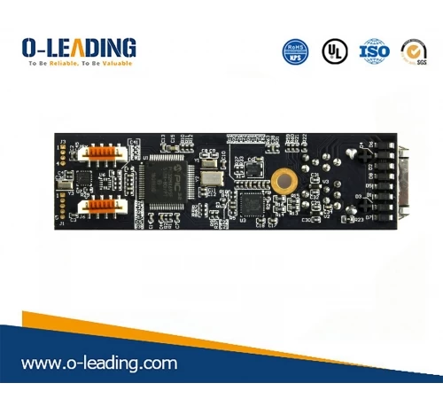
Power signal problem in pcb board design
o-leading.
o-leading.com
2019-03-08 16:28:33
Power signal integrity in pcb board design
In the meter pcb board, we are usually very concerned about the quality of the signal, but sometimes we are often limited to research signal lines, power supplies and ideals, although this can simplify the problem, but in high-speed design, simplification is no longer feasible. Although the direct result of circuit design is reflected in signal integrity, we cannot ignore the power integrity design. Because the integrity of the power supply directly affects the signal integrity of the final PCB. The integrity of the power supply and the integrity of the signal are closely related. In many cases, the main cause of signal distortion is the power supply system. For example, the ground rebound noise is too large, the design of the decoupling capacitor is not suitable, the circuit has serious influence, the division of multiple power/ground plane is not good, the design of the layer is unreasonable, and the current is not uniform.
1) Decoupling capacitor
We all know that adding some capacitance between the power supply and the ground can reduce the noise of the system, but how much capacitance does it increase? What is the inherent capacity of each capacitor? Is the position of each capacitor better? We are not serious Consider it, but it is based on the designer's experience and sometimes even less ability. In high-speed design, we must consider the parasitic capacitance parameters, quantitatively calculate the number of decoupling capacitors and the capacity value of each capacitor and the specific position of the placement to ensure the range of impedance control of the system. A basic principle is the decoupling capacitor. Need, one can not be less, overcapacity, do not like.
2) rebound
When the edge of a high-speed device is below 0.5 ns, the data exchange rate of the large-capacity data bus is so fast that when it is in the power supply layer, it is enough to affect the ripple of the signal, which can cause unstable power problems. When the current changes, the rate of change of the current increases, and the voltage of the ground increases with the voltage of the circuit. At this point, the ground plane (ground) is not an ideal zero level and the power supply is not ideal DC. As the gates of the switches increase, the ground bounce becomes more severe. For a 128-bit bus, there may be 50_100 I/O lines switching on the same clock. At this point, the power of the I/O driver and the inductance of the ground circuit must be as low as possible. Otherwise, the voltage brush will appear on the same ground. Ground reflections can be seen everywhere, such as chips, packages, connectors, or boards, which can bounce back, causing power system integrity problems.
From a technical point of view, the increase in equipment will only decrease, and the width of the bus will only increase. The only way to maintain an acceptable rebound is to reduce power supply and distribute inductance. For the chip, it means moving to an array chip, placing as much power as possible, as short as possible to reduce inductance. For encapsulation, it means that the moving layers are encapsulated, bringing the power ground plane closer, as in the BGA package. For connectors, it means using more feet or redesigning the connectors to have internal power and ground levels, such as link-based striplines. For a board, it means placing adjacent power supplies as close as possible to the ground plane. When the inductance is proportional to the length, the connection between the power supply and the ground will be minimized.
3) Power distribution system
Abstract Power integrity design is a very complex issue, but how to control the impedance between the power system (power and ground plane) is the key to the design. In theory, the lower the impedance of the power supply system, the lower the impedance, the lower the noise amplitude, and the lower the voltage loss. In the actual design, we can use the maximum voltage and power range to determine whether we want to reach the impedance target, and then adjust the relevant factors to make the target impedance of each part of the circuit's power supply system (frequency dependent) Close
Abstract Power integrity design is a very complex issue, but how to control the impedance between the power system (power and ground plane) is the key to the design. In theory, the lower the impedance of the power supply system, the lower the impedance, the lower the noise amplitude, and the lower the voltage loss. In the actual design, we can use the maximum voltage and power range to determine whether we want to reach the impedance target, and then adjust the relevant factors to make the target impedance of each part of the circuit's power supply system (frequency dependent) Close
O-Leading Supply Chain CO., LTD
TEL: + 86-752-8457668
Fax: + 86-4008892163-239121
+ 86-2028819702-239121