


PCB design and layout
Whether it is single-panel, double-panel, multi-layer board design, it was previously designed with protel, and the existing PADS, Allegro and other designs.
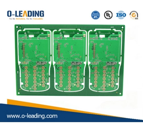
Impedance Control company china
The design of the printed circuit board is based on the circuit schematic diagram to achieve the functions required by the circuit designer. The design of the printed circuit board mainly refers to the layout design, which needs to consider the layout of the external connection, the optimized layout of the internal electronic components, the optimized layout of the metal wiring and the through hole, the electromagnetic protection, the heat dissipation and the like. Excellent layout design can save production costs and achieve good circuit performance and heat dissipation. Simple layout designs can be implemented manually, and complex layout designs need to be implemented with computer-aided design (CAD).
1 Overview
The purpose of this document is to illustrate the process and some considerations for the printed board design using the PADS printed board design software PowerPCB, to provide design specifications for designers of a working group to facilitate communication and mutual inspection between designers.
2 design process
The PCB design flow is divided into six steps: netlist input, rule setting, component layout, wiring, inspection, review, and output.
2.1 Netlist input
There are two ways to input the netlist. One is to use PowerLogic's OLE PowerPCB Connection function, select Send Netlist, and apply OLE function, you can keep the schematic and PCB diagram consistent at all times, and minimize the possibility of error. Another method is to load the netlist directly in the PowerPCB, select File->Import, and enter the netlist generated by the schematic.
2.2 Rule settings
If you have already set the PCB design rules in the schematic design stage, you don't need to set these rules anymore, because when you enter the netlist, the design rules have been entered into the PowerPCB with the netlist. If the design rules are modified, the schematic must be synchronized to ensure that the schematic and PCB are consistent. In addition to design rules and layer definitions, there are some rules that need to be set, such as Pad Stacks, which need to modify the size of standard vias. If the designer has created a new pad or via, be sure to add Layer 25.
note:
PCB design rules, layer definitions, via settings, and CAM output settings have been created as default startup files. The name is Default.stp. After the netlist is entered, the power network and ground are assigned to the power and ground layers according to the actual design conditions. And set other advanced rules. After all the rules are set, in PowerLogic, use the Rules From PCB function of OLE PowerPCB Connection to update the rule settings in the schematic to ensure that the rules of the schematic and the PCB are consistent.
2.3 Component layout
After the netlist is input, all the components will be placed at the zero point of the work area and overlapped. The next step is to separate the components and arrange them neatly according to some rules, that is, the layout of the components. PowerPCB offers two methods, manual layout and automatic layout.
2.3.1 Manual layout
1. The structural dimensions of the tool printed board are drawn with the board outline.
2. Disperse the components and arrange the components around the edge of the board.
3. Move the components one by one, rotate them, place them inside the edge of the board, and arrange them neatly according to certain rules.
2.3.2 Automatic layout
PowerPCB provides automatic layout and automatic local cluster layout, but for most designs, the effect is not ideal and is not recommended.
2.3.3 Precautions
a. The first principle of the layout is to ensure the routing rate of the wiring. Pay attention to the connection of the flying wires when moving the device, and put together the devices with the connection relationship.
b. Digital devices and analog devices should be separated and kept as far as possible
c. Decoupling capacitors as close as possible to the VCC of the device
d. Consider the future soldering when placing the device, not too dense
e. Increase the efficiency of the layout by using the Array and Union functions provided by the software.
2.4 wiring
There are also two ways to route, manual routing and automatic routing. The power wiring provided by PowerPCB is very powerful, including automatic push, online design rule checking (DRC), and automatic routing is performed by Specctra's routing engine. Usually these two methods are used together. The common steps are manual-automatic-manual.
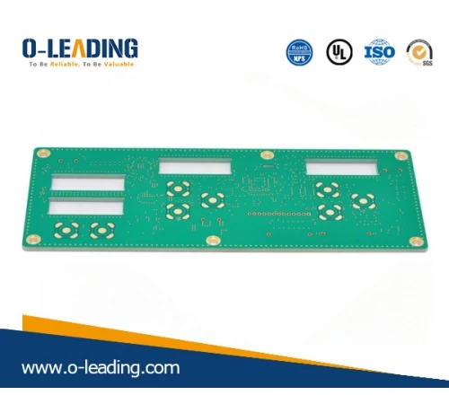
Blind-buried board supplier china
2.4.1 Manual wiring
1. Before auto-routing, first manually lay some important networks, such as high-frequency clocks, main power supplies, etc. These networks often have special requirements for trace distance, line width, line spacing, shielding, etc. Other special packages, Like BGA,
Automatic routing is difficult to lay out with rules, and manual wiring is also required.
2. After the automatic wiring, the wiring of the PCB should be adjusted by manual wiring.
2.4.2 Automatic wiring
After the manual routing is over, the remaining network is handed over to the autorouter. Select Tools->SPECCTRA, start the interface of the Specctra router, set the DO file, press Continue to start the automatic routing of the Specctra router. If the routing rate is 100% after the end, you can manually adjust the wiring; if not To 100%, there is a problem with the layout or manual wiring, and the layout or manual wiring needs to be adjusted until all the connections are made.
2.4.3 Precautions
a. Power cord and ground wire should be as thick as possible
b. Decoupling capacitors should be directly connected to VCC
c. When setting the Specctra DO file, first add the Protect all wires command to protect the hand cloth from being re-routed by the autorouter.
d. If there is a hybrid power layer, the layer should be defined as Split/mixed Plane, split before wiring, and after the wire is finished, use Pour Manager's Plane Connect for copper cladding.
e. Set all device pins to the thermal pad mode by setting Filter to Pins and selecting all pins.
Modify the properties and tick the Thermal option
f. Open the DRC option during manual routing, using Dynamic Route (Dynamic Route)
2.5 check
Items to be checked include Clearance, Connectivity, High Speed, and Plane. These items can be selected by Tools->Verify Design. If a high speed rule is set, it must be checked, otherwise this item can be skipped. Check for errors and you must modify the layout and routing.
note:
Some errors can be ignored. For example, some of the connectors' outlines are placed outside the board frame, and errors are detected when checking the spacing. In addition, each time the traces and vias are modified, the copper is re-copied once.
2.6 Review
Review according to the "PCB checklist", including design rules, layer definition, line width, spacing, pad, via settings; also focus on reviewing the rationality of device layout, power, ground network routing, high-speed clock network The wiring and shielding, the placement and connection of decoupling capacitors, etc. If the review fails, the designer must modify the layout and wiring. After passing the test, the reviewer and the designer separately sign.
2.7 Design output
The PCB design can be output to a printer or output illuminating file. The printer can print the PCB layer by layer, which is convenient for designers and reviewers to check; the lithography file is handed over to the board manufacturer to produce the printed board. The output of the light painting file is very important, which is related to the success or failure of this design. The following will focus on the precautions for outputting the light painting file.
a. The layers that need to be output are wiring layers (including top layer, bottom layer, intermediate wiring layer), power layer (including VCC layer and GND layer), silk screen layer (including top screen printing, bottom screen printing), solder mask (including top solder mask) And underlying solder mask), in addition to generate drilling files (NC Drill)
b. If the power layer is set to Split/Mixed, select Routing in the Document item of the Add Document window, and use the Pour Manager's Plane Connect to laminate the PCB before each output of the illuminating file; if set to CAM Plane, choose Plane. When setting the Layer item, add Layer25 and select Pads and Vias in the Layer 25 layer.
c. In the Device Settings window (press Device Setup), change the value of Aperture to 199.
d. Select the Board Outline when setting the Layer for each layer.
e. When setting the layer of the silkscreen layer, do not select Part Type, select the top (bottom) and silkscreen layers of Outline, Text, Line
f. When setting the layer of the solder mask, selecting the via hole means that no solder mask is added on the via hole, and the via hole is not selected to indicate the home solder mask, which is determined according to the specific situation.
g. When generating the drilling file, use the default settings of PowerPCB, do not make any changes.
h. After all the lithography files are output, open and print with CAM350, and the designer and reviewer will check according to the “PCB checklist”.