


PCB layout and routing techniques and pad copper design
1. Layout design Although Protel has the function of automatic layout, it can not fully meet the working needs of high-frequency circuits. It is often necessary to rely on the designer's experience to optimize the position of some components by manual layout according to the specific situation. , combined with automatic layout to complete the overall design of the PCB. Whether the layout is reasonable or not directly affects the life, stability, EMC (electromagnetic compatibility) of the product, etc., must be from the overall layout of the circuit board, the feasibility of the wiring and the manufacturability of the PCB, mechanical structure, heat dissipation, EMI (electromagnetic Comprehensive considerations such as interference), reliability, and signal integrity. Generally, the components in the fixed position related to the mechanical size are placed first, then the special and larger components are placed, and finally the small components are placed. At the same time, it is necessary to take into account the wiring requirements, the placement of high-frequency components should be as compact as possible, and the wiring of signal lines can be as short as possible, thereby reducing cross-interference of signal lines.
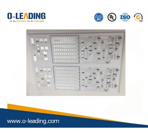
Multiple Flex-Rigid Board factory
1.1 Positioning of the positioning plug-in related to the mechanical size The power socket, the switch, the interface between the PCB, the indicator light, etc. are all positioning inserts related to the mechanical size. Usually, the interface between the power supply and the PCB is placed at the edge of the PCB and has a distance of 3 mm to 5 mm from the edge of the PCB; the indicator LED should be placed exactly as needed; the switch and some fine-tuning components, such as adjustable Inductors, adjustable resistors, etc. should be placed close to the edge of the PCB for easy adjustment and connection; components that need to be replaced frequently must be placed in a relatively small number of locations for easy replacement.
1.2 Special components are placed in high-power tubes, transformers, rectifiers and other heating devices. When generating heat in high-frequency conditions, more heat is generated. Therefore, ventilation and heat dissipation should be fully considered during layout, and such components should be placed on the PCB. A place where air is easy to circulate. High-power rectifiers and adjustment tubes should be equipped with heat sinks and away from the transformer. Electrolytic capacitors and other components that are afraid of heat should also be kept away from the heating device, otherwise the electrolyte will be baked, causing its resistance to increase, performance to deteriorate, and affecting the stability of the circuit. Components that are prone to failure, such as adjustment tubes, electrolytic capacitors, relays, etc., should also be considered for ease of maintenance when placed. For test points that often need to be measured, care should be taken to ensure that the test rods are easily accessible when arranging components. Since the 50 Hz leakage magnetic field is generated inside the power supply unit, it interferes with the low frequency amplifier when it is connected to some parts of the low frequency amplifier. Therefore, they must be isolated or shielded.
The amplifier stages are preferably arranged in a straight line according to the schematic diagram. The advantage of this arrangement is that the ground current of each stage is closed at the current stage and does not affect the operation of other circuits. The input and output stages should be as far apart as possible to reduce parasitic coupling interference between them. Considering the signal transmission relationship between the functional circuits of each unit, the low frequency circuit and the high frequency circuit should be separated, and the analog circuit and the digital circuit are separated. The integrated circuit should be placed in the center of the PCB so that the pins are easily wired to other devices. Devices such as inductors and transformers have magnetic coupling and should be placed orthogonally to each other to reduce magnetic coupling. In addition, they all have a strong magnetic field, and there should be a large space around them or magnetic shielding to reduce the influence on other circuits.
Appropriate high-frequency decoupling capacitors should be placed in the key parts of the PCB. For example, an electrolytic capacitor of 10μF to 100μF should be connected to the input end of the PCB power supply. A ceramic of about 0.01 pF should be connected near the power supply pin of the integrated circuit. Chip capacitor. Some circuits are also equipped with appropriate high frequency or low frequency chokes to reduce the effects between high and low frequency circuits. This should be considered in the schematic design and drawing, otherwise it will affect the performance of the circuit. The spacing of the components should be appropriate, and the spacing should be considered whether there is a possibility of breakdown or ignition between them. For amplifiers with push-pull circuits and bridge circuits, attention should be paid to the symmetry of the electrical parameters of the components and the symmetry of the structure, so that the distribution parameters of the symmetrical components are as uniform as possible. After the manual layout of the main components, the component locking method should be used so that these components do not move during automatic layout. That is, execute the Edit change command or select Locked in the Properties of the component to lock it no longer.
1.3 Placement of common components For ordinary components, such as resistors and capacitors, it should be considered from the aspects of neat arrangement of components, space occupation, wiring passability and convenience of soldering. the way.
2. The design and wiring of the wiring is the overall requirement for high-frequency PCB design on the basis of reasonable layout. Wiring includes both automatic routing and manual routing. Generally, regardless of the number of critical signal lines, these signal lines are manually wired first. After the wiring is completed, these signal lines are carefully inspected, fixed after inspection, and then automatically routed to other wirings. That is, the combination of manual and automatic wiring is used to complete the wiring of the PCB.
Special attention should be paid to the following aspects during the wiring process of high-frequency PCB.
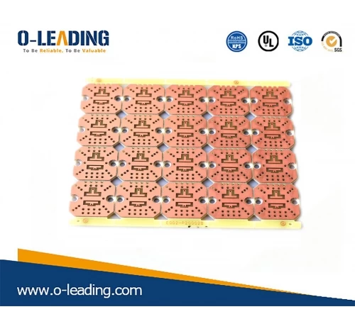
Impedance Control company china
2.1 The direction of the wiring The wiring of the circuit is preferably in full line according to the flow direction of the signal. It can be completed with a 45° fold line or a circular curve when turning. This can reduce the external emission and mutual coupling of high frequency signals. The wiring of the high-frequency signal lines should be as short as possible. According to the operating frequency of the circuit, the length of the signal line wiring is reasonably selected, which can reduce the distribution parameters and reduce the signal loss. When making a double panel, the wiring is preferably perpendicular, oblique or curved at the adjacent two levels. Avoid parallel to each other, which can reduce mutual interference and parasitic coupling. The high-frequency signal line and the low-frequency signal line should be separated as much as possible, and if necessary, shielding measures should be taken to prevent mutual interference. For receiving signal input that is weaker, it is easy to be interfered by external signals. You can use the ground wire to shield it and enclose it or shield the high-frequency connector. Parallel routing should be avoided on the same level, otherwise distribution parameters will be introduced, which will affect the circuit. If it is unavoidable, a grounded copper foil can be introduced between the two parallel lines to form an isolation line. In digital circuits, for differential signal lines, they should be routed in pairs, as far as possible, so that they are parallel, close to each other, and the length is not much different.
2.2 Form of Wiring During the wiring of the PCB, the minimum width of the trace is determined by the adhesion strength between the conductor and the insulating substrate and the current strength flowing through the conductor. When the thickness of the copper foil is 0.05 mm and the width is 1 mm to 1.5 mm, a current of 2 A can be passed. The temperature will not be higher than 3 °C. Except for some special traces, the width of other wiring on the same level should be as uniform as possible. The spacing of the wiring in the high frequency circuit will affect the size of the distributed capacitance and inductance, thereby affecting signal loss, circuit stability, and signal interference. In high-speed switching circuits, the spacing of the wires will affect the signal transmission time and the quality of the waveform. Therefore, the minimum spacing of the wiring should be greater than or equal to 0.5 mm. As long as the PCB layout is preferred, a wider line is preferred. The printed conductor should be spaced from the edge of the PCB by a certain distance (not less than the thickness of the board), which not only facilitates installation and machining, but also improves insulation performance. When wiring is encountered in a line that can only be connected by a large circle, the flying line should be used, that is, the short-line connection is directly used to reduce the interference caused by long-distance wiring. A circuit containing a magnetic sensing element is sensitive to a surrounding magnetic field, and a high-frequency circuit is susceptible to radiating electromagnetic waves when the wiring is bent. If a magnetic sensing element is placed in the PCB, the wiring corner should be kept at a certain distance therefrom. Wiring on the same level is not allowed to cross. For possible intersecting lines, it can be solved by "drilling" and "winding", that is, letting a certain lead "drill" from the gap under the pins of other devices such as resistors, capacitors, and triodes, or from a possible crossover. One end of the lead "wounds" past. In special cases, if the circuit is complex, to simplify the design, it is also possible to solve the crossover problem with wire bridging.
When the operating frequency of the high-frequency circuit is high, it is also necessary to consider the impedance matching and antenna effect of the wiring. Since the client changed the previous agreement at the end, it was required to change the layout to the right one according to the interface definition and placement position they defined. In fact, the area of the entire PCB is only 9cm x 6cm. It is difficult to change the overall layout of the board according to the requirements of the customer, so the core part of the board is not changed at the end, but the peripheral device is properly modified, mainly to complete the modification of the position and pin definition of the two connectors. However, the new layout obviously caused some trouble on the line. The originally smooth line became a little messy, the length of the line increased, and a lot of vias had to be used. The difficulty of the line was improved a lot.
2.3 Power cable and ground wire wiring requirements According to the different working current, try to increase the width of the power cable. The high-frequency PCB should use a large-area ground wire and be placed on the edge of the PCB as much as possible to reduce the interference of external signals on the circuit. At the same time, the ground wire of the PCB can be in good contact with the casing, so that the grounding voltage of the PCB is closer to Earth voltage. The grounding method should be selected according to the specific situation. It is different from the low-frequency circuit. The grounding wire of the high-frequency circuit should be grounded or multi-point grounded. The grounding wire is short and thick to minimize the ground impedance. 3 times the standard of working current. The ground wire of the speaker should be connected to the grounding point of the output stage of the PCB amplifier. Do not ground it at will. In the wiring process, some reasonable wiring should also be locked in time to avoid repeated wiring. That is, execute the EditselectNet command to select Locked in the pre-routed properties to lock it no longer.
3, the design of the pad and copper
3.1 Pads and Apertures Where the minimum spacing of the wiring is such that the electrical spacing of the design is not violated, the pad design should be large to ensure adequate loop width. Generally, the inner hole of the pad is slightly larger than the lead diameter of the component, and the design is too large to form a solder joint in the soldering. The pad outer diameter D is generally not less than (d + 1.2) mm, where d is the inner aperture of the pad. For some dense PCBs, the minimum value of the pad can be (d + 1.0) mm. The shape of the pad is usually set to a circular shape, but the pad of the integrated circuit for the DIP package is preferably in the shape of a racetrack, which can increase the area of the pad in a limited space and facilitate the soldering of the integrated circuit. The connection between the wiring and the pad should be smoothly transitioned. That is, when the width of the wiring entering the circular pad is smaller than the diameter of the circular pad, a teardrop design should be adopted. It should be noted that the size of the aperture d in the pad is different and should be considered according to the diameter of the actual component lead, such as component holes, mounting holes and slots. The hole pitch of the pad should also be considered according to the installation method of the actual components. For example, resistors, diodes, tubular capacitors and other components have "vertical" and "horizontal" mounting modes. The pitch of the two methods is different. In addition, the pad pitch is designed to take into account the minimum gap requirements between components, especially the gap between special components needs to be ensured by the pitch between the pads.
In high-frequency PCBs, the number of vias should also be minimized, which reduces the distributed capacitance and increases the mechanical strength of the PCB. In short, in the design of high-frequency PCB, the design of the pad and its shape, aperture and pitch should be considered in consideration of its particularity and the requirements of the production process. Adopting a standardized design can not only reduce product costs, but also improve production efficiency while ensuring product quality.
3.2 The main purpose of copper-clad copper is to improve the anti-interference ability of the circuit. At the same time, it has great benefits for PCB heat dissipation and PCB strength. The copper grounding can also play a shielding role. However, it is not possible to use a large-area strip of copper foil because it will generate a large amount of heat when the PCB is used for a long time. At this time, the strip-shaped copper foil is liable to expand and fall off. Therefore, it is preferable to use a grid when applying copper. The copper foil is connected to the grounding network of the circuit, so that the grid will have a better shielding effect. The size of the grid is determined by the interference frequency to be shielded. After completing the design of the wiring, pads, and vias, DRC (Design Rule Check) should be performed. The difference between the designed map and the defined rules is detailed in the inspection results, and the network that does not meet the requirements can be found. However, the DRC should be parameterized before wiring to run the DRC, that is, execute the ToolsDesign Rule Check command.
O-Leading Supply Chain CO., LTD
TEL: + 86-752-8457668
Fax: + 86-4008892163-239121
+ 86-2028819702-239121