


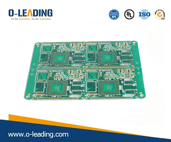
PCB board plating via performance evaluation for 5G applications
Due to the presence of microspheres, the appearance of circuit-processed structures, such as metallized vias (PTH) from one conductive layer to another, appears to be more traditional than conventional circuit board materials that do not use such special dielectric fillers. The formed metallized vias are made rougher. It may seem like this, or is there any other concern, after all, because the circuit board with hollow microsphere filler is very rough when making metallized vias. However, a series of studies have shown that the effect of hollow microsphere fillers on metallized vias is purely surface appearance, both at RF frequencies and at millimeter-wave frequencies of 5G wireless networks, and it does not affect the circuit. Performance or reliability of metallized vias.
Halogen free pcb factory china.
The texture of the wall surface of the metallized vias of all circuits has different subtle differences, even when comparing the roughness of the surface of the hole wall of the same board. Since the drilling process involves a number of factors, the surface of the wall of the metallized via may vary from hole to hole. In materials with microsphere fillers, the drill bit may or may not affect the microsphere filler, resulting in a difference. When the drill bit impacts and breaks the hollow sphere, the copper plating of the via will grow along the contour of the broken sphere, and the surface of the pore wall will no longer be smooth and flat.
Printed circuit boards supplier.
With the increasing demand for high frequency circuit materials in a wide frequency range in 5G wireless networks, it is very meaningful to know whether the surface roughness of metallized vias in the board material with hollow microsphere fillers has an impact on circuit performance, because There is no such filler in conventional circuit board materials.
The test circuit is based on a microstrip transmission line structure with a via in the middle of the circuit for conductor and signal transitions from the top copper layer of the dielectric substrate material to the bottom copper layer. The length of the test circuit is basically about 2 inches. We also used other high frequency transmission line technologies as a reference to evaluate the effect of metallized via wall surface roughness, including 8-inch and 2-inch long microstrip circuits without signal vias, and 8-inch and 2" long grounded coplanar waveguide (GCPW) circuit without through holes.